参数资料
| 型号: | LTC1297BCN8 |
| 厂商: | Linear Technology |
| 文件页数: | 9/24页 |
| 文件大小: | 0K |
| 描述: | IC DATA ACQ SYSTEM 12BIT 8-DIP |
| 标准包装: | 50 |
| 类型: | 数据采集系统(DAS) |
| 分辨率(位): | 12 b |
| 采样率(每秒): | 60k |
| 数据接口: | 串行,并联 |
| 电压电源: | 单电源 |
| 电源电压: | 5V |
| 工作温度: | 0°C ~ 70°C |
| 安装类型: | 通孔 |
| 封装/外壳: | 8-DIP(0.300",7.62mm) |
| 供应商设备封装: | 8-PDIP |
| 包装: | 管件 |
17
LTC1292/LTC1297
12927fb
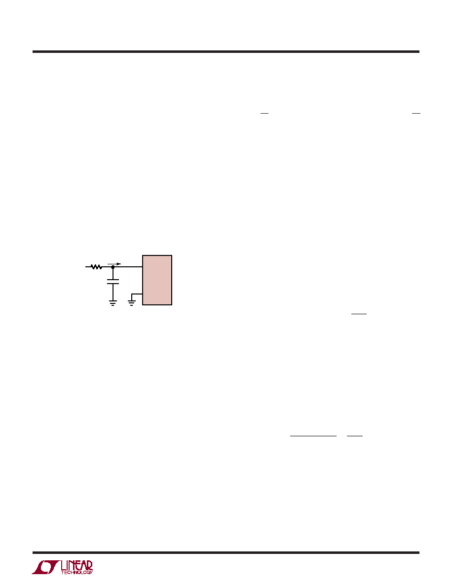
RC Input Filtering
It is possible to filter the inputs with an RC network as
shown in Figure 15. For large values of CF (e.g., 1F) the
capacitive input switching currents are averaged into a net
DC current. A filter should be chosen with a small resistor
and large capacitor to prevent DC drops across the resistor.
The magnitude of the DC current is approximately IDC =
100pF
× VIN/tCYC and is roughly proportional to VIN. When
running the LTC1292(LTC1297) at the minimum cycle
time of 16.5
s (20s), the input current equals 30A
(25
A) at VIN = 5V. Here a filter resistor of 4 (5) will
cause 0.1LSB of full scale error. If a large filter resistor
must be used, errors can be reduced by increasing the
cycle time as shown in the typical performance
characteristics curve Maximum Filter Resistor vs Cycle
Time.
Figure 15. RC Input Filtering
curve of S&H Acquisition Time vs Source Resistance). The
input voltage is sampled during the tSMPL time as shown
in Figure 11. The sampling interval begins at the rising
edge of CS for the LTC1292, and at the falling edge of CS
for the LTC1297, and continues until the falling edge of the
CLK before the conversion begins. On this falling edge the
S&H goes into the hold mode and the conversion begins.
Differential Input
With a differential input the A/D no longer converts a single
voltage but converts the difference between two voltages.
The voltage on the +IN pin is sampled and held and can be
rapidly time-varying as in single-ended mode. The voltage
on the –IN pin must remain constant and be free of noise
and ripple throughout the conversion time. Otherwise the
differencing operation will not be done accurately. The
conversion time is 12 CLK cycles. Therefore a change in
the –IN input voltage during this interval can cause
conversion errors. For a sinusoidal voltage on the –IN
input this error would be:
Vf
V
f
ERROR MAX
IN PEAK
CLK
(
)
(– )
=
()
2
12
π
Where f(–IN) is the frequency of the –IN input voltage,
VPEAK is its peak amplitude and fCLK is the frequency of the
CLK. Usually VERROR will not be significant. For a 60Hz
signal on the –IN input to generate a 0.25LSB error
(300
V) with the converter running at CLK = 1MHz, its
peak value would have to be 66mV. Rearranging the above
equation the maximum sinusoidal signal that can be
digitized to a given accuracy is given as:
f
V
f
IN MAX
ERROR MAX
PEAK
CLK
(– )
()
=
π
2
12
For 0.25LSB error (300
V) the maximum input sinusoid
with a 5V peak amplitude that can be digitized is 0.8Hz.
Reference Input
The voltage on the reference input of the LTC1292/
LTC1297 determine the voltage span of the A/D con-
verter. The reference input has transient capacitive
Input Leakage Current
Input leakage currents also can create errors if the source
resistance gets too large. For example, the maximum input
leakage specification of 1
A flowing through a source
resistance of 1k will cause a voltage drop of 1mV or
0.8LSB. This error will be much reduced at lower
temperatures because leakage drops rapidly (see typical
performance characteristics curve Input Channel Leakage
Current vs Temperature).
SAMPLE-AND-HOLD
Single-Ended Input
The LTC1292/LTC1297 provide a built-in sample-and-
hold (S&H) function on the +IN input for signals acquired
in the single-ended mode (–IN pin grounded). The sample-
and-hold allows the LTC1292/LTC1297 to convert rapidly
varying signals (see typical performance characteristics
RFILTER
CFILTER
LTC1292/7 F15
LTC1292
LTC1297
“+”
“–”
IDC
VIN
U
S
A
O
PPLICATI
WU
U
I FOR ATIO
相关PDF资料 |
PDF描述 |
|---|---|
| VI-B1K-IU-F2 | CONVERTER MOD DC/DC 40V 200W |
| LTC6905CS5-96#TRPBF | IC OSC SILICON 96MHZ TSOT23-5 |
| VI-B1K-IU-F1 | CONVERTER MOD DC/DC 40V 200W |
| AD7890BRZ-10 | IC DAS 12BIT 8CH 24-SOIC |
| LTC6905CS5-133#TRMPBF | IC OSC SILICON 133MHZ TSOT23-5 |
相关代理商/技术参数 |
参数描述 |
|---|---|
| LTC1297BCN8#PBF | 功能描述:IC DATA ACQ SYSTEM 12BIT 8-DIP RoHS:是 类别:集成电路 (IC) >> 数据采集 - ADCs/DAC - 专用型 系列:- 产品培训模块:Lead (SnPb) Finish for COTS Obsolescence Mitigation Program 标准包装:50 系列:- 类型:数据采集系统(DAS) 分辨率(位):16 b 采样率(每秒):21.94k 数据接口:MICROWIRE?,QSPI?,串行,SPI? 电压电源:模拟和数字 电源电压:1.8 V ~ 3.6 V 工作温度:-40°C ~ 85°C 安装类型:表面贴装 封装/外壳:40-WFQFN 裸露焊盘 供应商设备封装:40-TQFN-EP(6x6) 包装:托盘 |
| LTC1297CCJ8 | 制造商:Linear Technology 功能描述:ADC Single SAR 50ksps 12-bit Serial 8-Pin CDIP |
| LTC1297CCN8 | 功能描述:IC DATA ACQ SYSTEM 12BIT 8-DIP RoHS:否 类别:集成电路 (IC) >> 数据采集 - ADCs/DAC - 专用型 系列:- 产品培训模块:Lead (SnPb) Finish for COTS Obsolescence Mitigation Program 标准包装:50 系列:- 类型:数据采集系统(DAS) 分辨率(位):16 b 采样率(每秒):21.94k 数据接口:MICROWIRE?,QSPI?,串行,SPI? 电压电源:模拟和数字 电源电压:1.8 V ~ 3.6 V 工作温度:-40°C ~ 85°C 安装类型:表面贴装 封装/外壳:40-WFQFN 裸露焊盘 供应商设备封装:40-TQFN-EP(6x6) 包装:托盘 |
| LTC1297CCN8#PBF | 功能描述:IC DATA ACQ SYSTEM 12BIT 8-DIP RoHS:是 类别:集成电路 (IC) >> 数据采集 - ADCs/DAC - 专用型 系列:- 产品培训模块:Lead (SnPb) Finish for COTS Obsolescence Mitigation Program 标准包装:50 系列:- 类型:数据采集系统(DAS) 分辨率(位):16 b 采样率(每秒):21.94k 数据接口:MICROWIRE?,QSPI?,串行,SPI? 电压电源:模拟和数字 电源电压:1.8 V ~ 3.6 V 工作温度:-40°C ~ 85°C 安装类型:表面贴装 封装/外壳:40-WFQFN 裸露焊盘 供应商设备封装:40-TQFN-EP(6x6) 包装:托盘 |
| LTC1297CCN8PBF | 制造商:Linear Technology 功能描述:LTC1297CCN8PBF |
发布紧急采购,3分钟左右您将得到回复。