参数资料
| 型号: | LTC1297BCN8 |
| 厂商: | Linear Technology |
| 文件页数: | 8/24页 |
| 文件大小: | 0K |
| 描述: | IC DATA ACQ SYSTEM 12BIT 8-DIP |
| 标准包装: | 50 |
| 类型: | 数据采集系统(DAS) |
| 分辨率(位): | 12 b |
| 采样率(每秒): | 60k |
| 数据接口: | 串行,并联 |
| 电压电源: | 单电源 |
| 电源电压: | 5V |
| 工作温度: | 0°C ~ 70°C |
| 安装类型: | 通孔 |
| 封装/外壳: | 8-DIP(0.300",7.62mm) |
| 供应商设备封装: | 8-PDIP |
| 包装: | 管件 |
16
LTC1292/LTC1297
12927fb
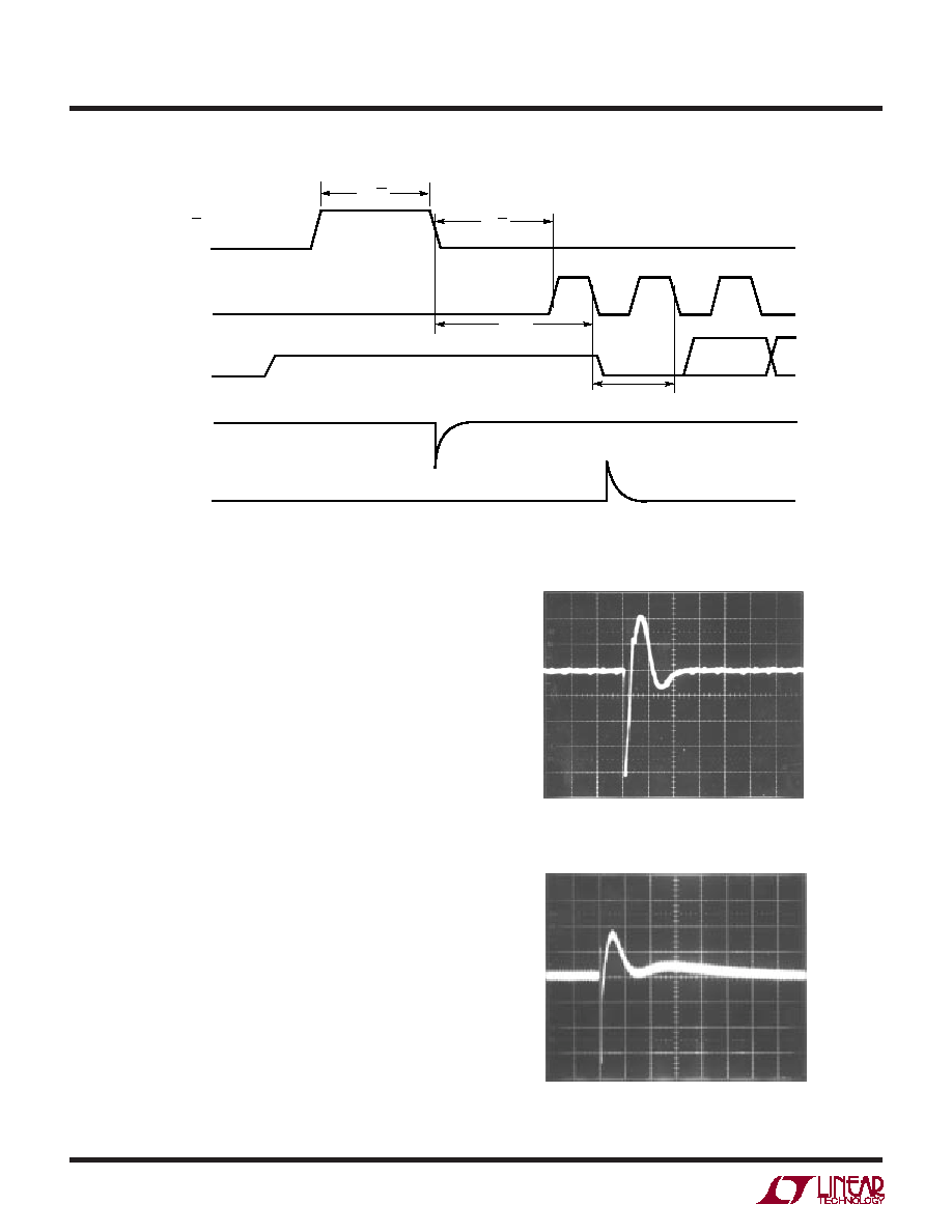
Figure 12. “+” and “–” Input Settling Windows for the LTC1297
“–” input voltage be free of noise and settle completely
during the first CLK cycle of the conversion. Minimizing
RSOURCE– and C2 will improve settling time. If large “–”
input source resistance must be used the time can be
extended by using a slower CLK frequency. At the maximum
CLK frequency of 1MHz, RSOURCE– < 250and C2 < 20pF
will provide adequate settling.
Input Op Amps
When driving the analog inputs with an op amp it is
important that the op amp settles within the allowed time
(see Figures 11a, 11b, 11c and 12). Again the “+” and “–
” input sampling times can be extended as described
above to accommodate slower op amps. Most op amps
including the LT1797 and LT1677 single supply op amps
can be made to settle well even with the minimum settling
windows of 3.0
s for the LTC1292 or 6.0s for the
LTC1297 (“+” input) and 1
s (“–” input) that occurs at the
maximum clock rate of 1MHz. Figures 13 and 14 show
examples of both adequate and poor op amp settling.
VERTICAL:
5mV/DIV
HORIZONTAL: 500ns/DIV
HORIZONTAL: 20
s/DIV
Figure 13. Adequate Settling of Op Amp Driving Analog Input
VERTICAL:
5mV/DIV
Figure 14. Poor Op Amp Settling Can Cause A/D Errors
U
S
A
O
PPLICATI
WU
U
I FOR ATIO
DOUT
CLK
B11
HI-Z
B10
LTC1292/7 F12
CS
1ST BIT TEST (–) INPUT MUST
SETTLE DURING THIS TIME
tWHCS
tSMPL
(+) INPUT MUST SETTLE
DURING THIS TIME
(+) INPUT
(–) INPUT
tsuCS
相关PDF资料 |
PDF描述 |
|---|---|
| VI-B1K-IU-F2 | CONVERTER MOD DC/DC 40V 200W |
| LTC6905CS5-96#TRPBF | IC OSC SILICON 96MHZ TSOT23-5 |
| VI-B1K-IU-F1 | CONVERTER MOD DC/DC 40V 200W |
| AD7890BRZ-10 | IC DAS 12BIT 8CH 24-SOIC |
| LTC6905CS5-133#TRMPBF | IC OSC SILICON 133MHZ TSOT23-5 |
相关代理商/技术参数 |
参数描述 |
|---|---|
| LTC1297BCN8#PBF | 功能描述:IC DATA ACQ SYSTEM 12BIT 8-DIP RoHS:是 类别:集成电路 (IC) >> 数据采集 - ADCs/DAC - 专用型 系列:- 产品培训模块:Lead (SnPb) Finish for COTS Obsolescence Mitigation Program 标准包装:50 系列:- 类型:数据采集系统(DAS) 分辨率(位):16 b 采样率(每秒):21.94k 数据接口:MICROWIRE?,QSPI?,串行,SPI? 电压电源:模拟和数字 电源电压:1.8 V ~ 3.6 V 工作温度:-40°C ~ 85°C 安装类型:表面贴装 封装/外壳:40-WFQFN 裸露焊盘 供应商设备封装:40-TQFN-EP(6x6) 包装:托盘 |
| LTC1297CCJ8 | 制造商:Linear Technology 功能描述:ADC Single SAR 50ksps 12-bit Serial 8-Pin CDIP |
| LTC1297CCN8 | 功能描述:IC DATA ACQ SYSTEM 12BIT 8-DIP RoHS:否 类别:集成电路 (IC) >> 数据采集 - ADCs/DAC - 专用型 系列:- 产品培训模块:Lead (SnPb) Finish for COTS Obsolescence Mitigation Program 标准包装:50 系列:- 类型:数据采集系统(DAS) 分辨率(位):16 b 采样率(每秒):21.94k 数据接口:MICROWIRE?,QSPI?,串行,SPI? 电压电源:模拟和数字 电源电压:1.8 V ~ 3.6 V 工作温度:-40°C ~ 85°C 安装类型:表面贴装 封装/外壳:40-WFQFN 裸露焊盘 供应商设备封装:40-TQFN-EP(6x6) 包装:托盘 |
| LTC1297CCN8#PBF | 功能描述:IC DATA ACQ SYSTEM 12BIT 8-DIP RoHS:是 类别:集成电路 (IC) >> 数据采集 - ADCs/DAC - 专用型 系列:- 产品培训模块:Lead (SnPb) Finish for COTS Obsolescence Mitigation Program 标准包装:50 系列:- 类型:数据采集系统(DAS) 分辨率(位):16 b 采样率(每秒):21.94k 数据接口:MICROWIRE?,QSPI?,串行,SPI? 电压电源:模拟和数字 电源电压:1.8 V ~ 3.6 V 工作温度:-40°C ~ 85°C 安装类型:表面贴装 封装/外壳:40-WFQFN 裸露焊盘 供应商设备封装:40-TQFN-EP(6x6) 包装:托盘 |
| LTC1297CCN8PBF | 制造商:Linear Technology 功能描述:LTC1297CCN8PBF |
发布紧急采购,3分钟左右您将得到回复。