参数资料
| 型号: | LTC1297BCN8 |
| 厂商: | Linear Technology |
| 文件页数: | 15/24页 |
| 文件大小: | 0K |
| 描述: | IC DATA ACQ SYSTEM 12BIT 8-DIP |
| 标准包装: | 50 |
| 类型: | 数据采集系统(DAS) |
| 分辨率(位): | 12 b |
| 采样率(每秒): | 60k |
| 数据接口: | 串行,并联 |
| 电压电源: | 单电源 |
| 电源电压: | 5V |
| 工作温度: | 0°C ~ 70°C |
| 安装类型: | 通孔 |
| 封装/外壳: | 8-DIP(0.300",7.62mm) |
| 供应商设备封装: | 8-PDIP |
| 包装: | 管件 |
22
LTC1292/LTC1297
12927fb
U
S
A
O
PPLICATI
WU
U
I FOR ATIO
LSB
(B0)
LSB-FIRST DATA
(B1)
MSB
(B11)
NULL
BIT
VERTICAL: 5V/DIV
HORIZONTAL: 2
s/DIV
CLK
CS
D
OUT
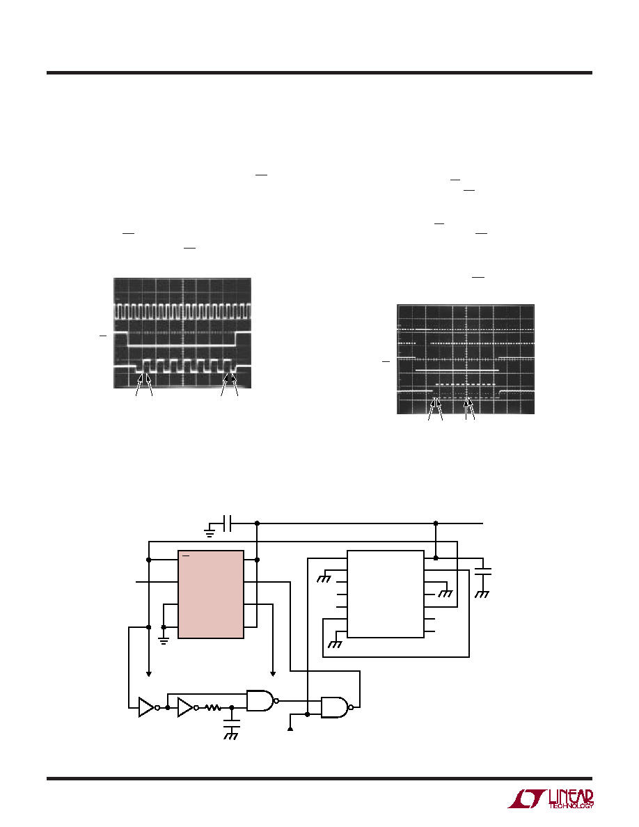
A “Quick Look” Circuit for the LTC1297
A circuit similar to the one used for the LTC1292 can be
used for the LTC1297(Figure 28). A one shot has been
generated with NAND gates, a resistor and capacitor to
satisfy the setup time tsuCS. This can be eliminated if a
slower clock is used. When CS goes low the one shot is
triggered. This turns off the clock to the LTC1297 for a
fixed time to meet tsuCS. Once the clock starts DOUT is
shifted out one bit at a time. CS is driven at 1/64 the
clock rate by the 74HC393. The output data from the
DOUT pin can be viewed on an oscilloscope that is set to
trigger on the falling edge of CS. See Figure 29.
CS
CLK
D
OUT
NULL
BIT
MSB
(B11)
LSB-FIRST DATA
(B1)
LSB
(B0)
VERTICAL: 5V/DIV
HORIZONTAL: 5
s/DIV
Figure 29. Scope Trace of the LTC1297 “Quick Look”
Circuit Showing A/D Output 101010101010 (AAAHEX)
Figure 27. Scope Trace of the LTC1292 “Quick Look”
Circuit Showing A/D Output 101010101010 (AAAHEX)
Figure 28. “Quick Look” Circuit for the LTC1297
TO OSCILLOSCOPE
LTC1292/7 F28
0.1
F
VIN
f/64
5V
340
22
F
TANTALUM
VCC
CLK
DOUT
VREF
CS
+IN
–IN
GND
LTC1297
74HC393
A1
CLR1
1QA
1QB
1QC
1QD
GND
VCC
A2
CLR2
2QA
2QB
2QC
2QD
+
f
0.02
F
CLOCK IN 1MHz
A “Quick Look” Circuit for the LTC1292
Users can get a quick look at the function and timing of
the LTC1292 by using the “Quick Look” circuit in Figure
26. VREF is tied to VCC. VIN is applied to the +IN input
and the –IN input is tied to the ground plane. CS is driven
at 1/32 the clock rate by the CD4520 and DOUT outputs
the data. The output data from the DOUT pin can be
viewed on an oscilloscope that is set up to trigger on the
falling edge of CS (Figure 27). Note the LSB data is
partially clocked out before CS goes high.
相关PDF资料 |
PDF描述 |
|---|---|
| VI-B1K-IU-F2 | CONVERTER MOD DC/DC 40V 200W |
| LTC6905CS5-96#TRPBF | IC OSC SILICON 96MHZ TSOT23-5 |
| VI-B1K-IU-F1 | CONVERTER MOD DC/DC 40V 200W |
| AD7890BRZ-10 | IC DAS 12BIT 8CH 24-SOIC |
| LTC6905CS5-133#TRMPBF | IC OSC SILICON 133MHZ TSOT23-5 |
相关代理商/技术参数 |
参数描述 |
|---|---|
| LTC1297BCN8#PBF | 功能描述:IC DATA ACQ SYSTEM 12BIT 8-DIP RoHS:是 类别:集成电路 (IC) >> 数据采集 - ADCs/DAC - 专用型 系列:- 产品培训模块:Lead (SnPb) Finish for COTS Obsolescence Mitigation Program 标准包装:50 系列:- 类型:数据采集系统(DAS) 分辨率(位):16 b 采样率(每秒):21.94k 数据接口:MICROWIRE?,QSPI?,串行,SPI? 电压电源:模拟和数字 电源电压:1.8 V ~ 3.6 V 工作温度:-40°C ~ 85°C 安装类型:表面贴装 封装/外壳:40-WFQFN 裸露焊盘 供应商设备封装:40-TQFN-EP(6x6) 包装:托盘 |
| LTC1297CCJ8 | 制造商:Linear Technology 功能描述:ADC Single SAR 50ksps 12-bit Serial 8-Pin CDIP |
| LTC1297CCN8 | 功能描述:IC DATA ACQ SYSTEM 12BIT 8-DIP RoHS:否 类别:集成电路 (IC) >> 数据采集 - ADCs/DAC - 专用型 系列:- 产品培训模块:Lead (SnPb) Finish for COTS Obsolescence Mitigation Program 标准包装:50 系列:- 类型:数据采集系统(DAS) 分辨率(位):16 b 采样率(每秒):21.94k 数据接口:MICROWIRE?,QSPI?,串行,SPI? 电压电源:模拟和数字 电源电压:1.8 V ~ 3.6 V 工作温度:-40°C ~ 85°C 安装类型:表面贴装 封装/外壳:40-WFQFN 裸露焊盘 供应商设备封装:40-TQFN-EP(6x6) 包装:托盘 |
| LTC1297CCN8#PBF | 功能描述:IC DATA ACQ SYSTEM 12BIT 8-DIP RoHS:是 类别:集成电路 (IC) >> 数据采集 - ADCs/DAC - 专用型 系列:- 产品培训模块:Lead (SnPb) Finish for COTS Obsolescence Mitigation Program 标准包装:50 系列:- 类型:数据采集系统(DAS) 分辨率(位):16 b 采样率(每秒):21.94k 数据接口:MICROWIRE?,QSPI?,串行,SPI? 电压电源:模拟和数字 电源电压:1.8 V ~ 3.6 V 工作温度:-40°C ~ 85°C 安装类型:表面贴装 封装/外壳:40-WFQFN 裸露焊盘 供应商设备封装:40-TQFN-EP(6x6) 包装:托盘 |
| LTC1297CCN8PBF | 制造商:Linear Technology 功能描述:LTC1297CCN8PBF |
发布紧急采购,3分钟左右您将得到回复。