- 您现在的位置:买卖IC网 > PDF目录10667 > LTC1408CUH#PBF (Linear Technology)IC ADC 14BIT 600KSPS 32-QFN PDF资料下载
参数资料
| 型号: | LTC1408CUH#PBF |
| 厂商: | Linear Technology |
| 文件页数: | 10/20页 |
| 文件大小: | 0K |
| 描述: | IC ADC 14BIT 600KSPS 32-QFN |
| 标准包装: | 73 |
| 位数: | 14 |
| 采样率(每秒): | 600k |
| 数据接口: | 串行 |
| 转换器数目: | 1 |
| 功率耗散(最大): | 15mW |
| 电压电源: | 模拟和数字 |
| 工作温度: | 0°C ~ 70°C |
| 安装类型: | 表面贴装 |
| 封装/外壳: | 32-WFQFN 裸露焊盘 |
| 供应商设备封装: | 32-QFN 裸露焊盘(5x5) |
| 包装: | 管件 |
| 输入数目和类型: | 12 个单端,单极;12 个单端,双极;6 个差分,单极;6 个差分,双极 |
| 产品目录页面: | 1346 (CN2011-ZH PDF) |
| 配用: | DC887A-ND - BOARD SAR ADC LTC1408 |
18
LTC1408
1408fa
APPLICATIO S I FOR ATIO
WU
UU
1408 F06
3
30
32
1
2
3-WIRE SERIAL
INTERFACE LINK
OVDD
CONV
SCK
LTC1408
SDO
VCC
BFSR
BCLKR
TMS320C54x
BDR
OGND
31
DGND
CONV
0V TO 3V LOGIC SWING
CLK
5V
3V
B13
B12
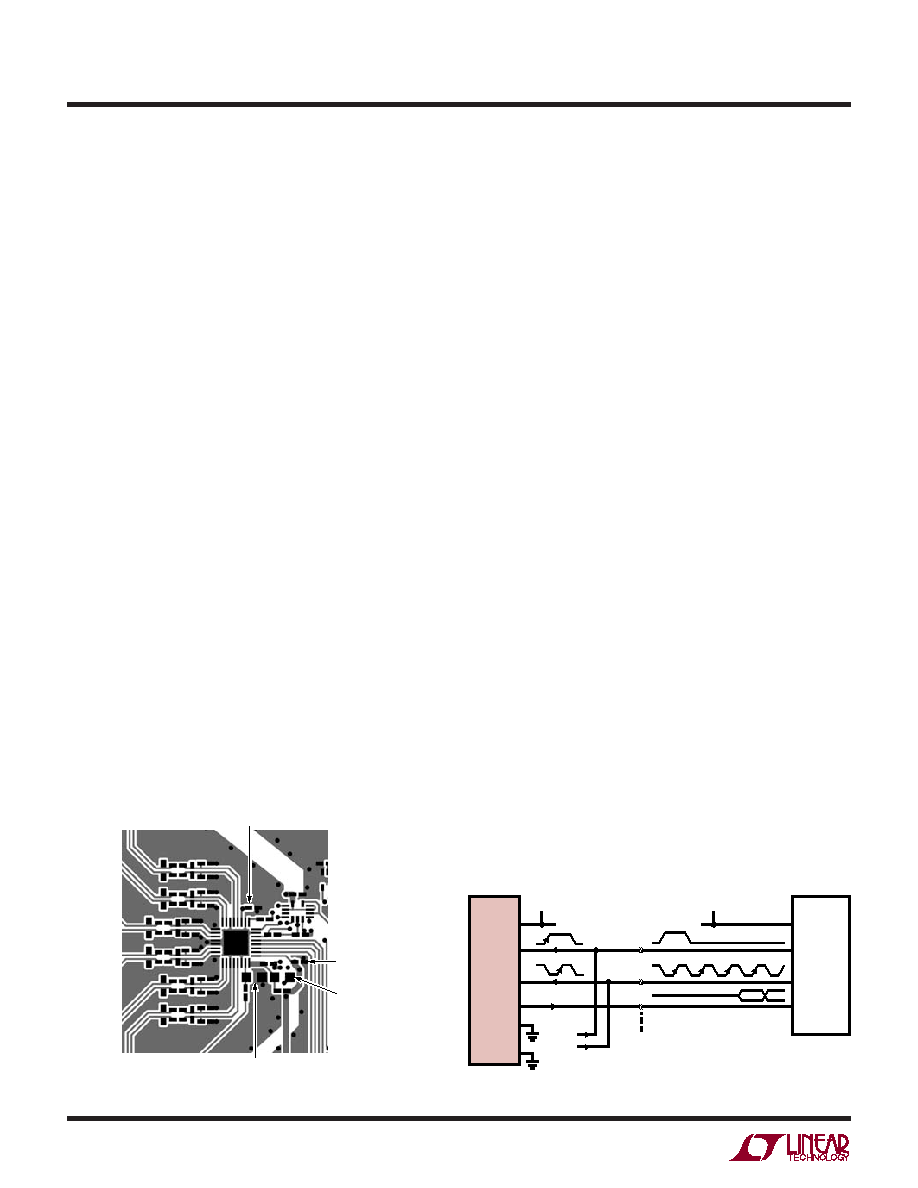
Figure 7. DSP Serial Interface to TMS320C54x
BOARD LAYOUT AND BYPASSING
Wire wrap boards are not recommended for high resolu-
tion and/or high speed A/D converters. To obtain the best
performance from the LTC1408, a printed circuit board
with ground plane is required. Layout for the printed circuit
board should ensure that digital and analog signal lines are
separated as much as possible. In particular, care should
be taken not to run any digital track alongside an analog
signal track. If optimum phase match between the inputs
is desired, the length of the twelve input wires of the six
input channels should be kept matched. But each pair of
input wires to the six input channels should be kept
separated by a ground trace to avoid high frequency
crosstalk between channels.
High quality tantalum and ceramic bypass capacitors should
be used at the VCC, VDD and VREF pins as shown in the Block
Diagram on the first page of this data sheet. For optimum
performance, a 10
F surface mount tantalum capacitor
with a 0.1
F ceramic is recommended for the VCC,VDD and
VREF pins. Alternatively, 10F ceramic chip capacitors such
as X5R or X7R may be used. The capacitors must be lo-
cated as close to the pins as possible. The traces connect-
ing the pins and the bypass capacitors must be kept short
and should be made as wide as possible. The VCC and VDD
bypass capacitor returns to the ground plane and the VREF
bypass capacitor returns to the Pin 22. Care should be
taken to place the 0.1
F VCC and VDD bypass capacitor as
close to Pins 24 and 25 as possible.
Figure 6. Recommended Layout
Figure 6 shows the recommended system ground connec-
tions. All analog circuitry grounds should be terminated at
the LTC1408 Exposed Pad. The ground return from the
LTC1408 to the power supply should be low impedance for
noise-free operation. The Exposed Pad of the 32-pin QFN
package is also internally tied to the ground pads. The
Exposed Pad should be soldered on the PC board to reduce
ground connection inductance. All ground pins (GND,
DGND, OGND) must be connected directly to the same
ground plane under the LTC1408.
VDD BYPASS,
0.1
F, 0402
OVDD BYPASS,
0.1
F, 0402
VREF BYPASS,
10
F, 0805
VCC BYPASS,
0.1
F, 0402 AND
10
F, 0805
HARDWARE INTERFACE TO TMS320C54x
The LTC1408 is a serial output ADC whose interface has
been designed for high speed buffered serial ports in fast
digital signal processors (DSPs). Figure 7 shows an
example of this interface using a TMS320C54X.
The buffered serial port in the TMS320C54x has direct
access to a 2kB segment of memory. The ADC’s serial data
can be collected in two alternating 1kB segments, in real
time, at the full 600ksps conversion rate of the LTC1408.
The DSP assembly code sets frame sync mode at the BFSR
pin to accept an external positive going pulse and the serial
clock at the BCLKR pin to accept an external positive edge
clock. Buffers near the LTC1408 may be added to drive
long tracks to the DSP to prevent corruption of the signal
to LTC1408. This configuration is adequate to traverse a
typical system board, but source resistors at the buffer
outputs and termination resistors at the DSP, may be
needed to match the characteristic impedance of very long
transmission lines. If you need to terminate the SDO
transmission line, buffer it first with one or two 74ACxx
gates. The TTL threshold inputs of the DSP port respond
properly to the 3V swing used with the LTC1408.
相关PDF资料 |
PDF描述 |
|---|---|
| MC10E1651FNR2G | IC COMPARATOR DUAL ECL 20-PLCC |
| AD9204BCPZ-80 | IC ADC 10BIT 80MSPS DL 64LFCSP |
| LTC2226IUH#PBF | IC ADC 12BIT 25MSPS SAMPL 32-QFN |
| MC10E1652FNR2G | IC COMPARATOR DUAL ECL 20PLCC |
| AD7714ANZ-5 | IC ADC SIGNAL COND 5V 24-DIP |
相关代理商/技术参数 |
参数描述 |
|---|---|
| LTC1408IUH#PBF | 功能描述:IC ADC 14BIT 600KSPS 32-QFN RoHS:是 类别:集成电路 (IC) >> 数据采集 - 模数转换器 系列:- 标准包装:1 系列:microPOWER™ 位数:8 采样率(每秒):1M 数据接口:串行,SPI? 转换器数目:1 功率耗散(最大):- 电压电源:模拟和数字 工作温度:-40°C ~ 125°C 安装类型:表面贴装 封装/外壳:24-VFQFN 裸露焊盘 供应商设备封装:24-VQFN 裸露焊盘(4x4) 包装:Digi-Reel® 输入数目和类型:8 个单端,单极 产品目录页面:892 (CN2011-ZH PDF) 其它名称:296-25851-6 |
| LTC1408IUH#TRPBF | 功能描述:IC ADC 14BIT 600KSPS 32-QFN RoHS:是 类别:集成电路 (IC) >> 数据采集 - 模数转换器 系列:- 标准包装:1,000 系列:- 位数:12 采样率(每秒):300k 数据接口:并联 转换器数目:1 功率耗散(最大):75mW 电压电源:单电源 工作温度:0°C ~ 70°C 安装类型:表面贴装 封装/外壳:24-SOIC(0.295",7.50mm 宽) 供应商设备封装:24-SOIC 包装:带卷 (TR) 输入数目和类型:1 个单端,单极;1 个单端,双极 |
| LTC1408IUH-12#PBF | 功能描述:IC ADC 12BIT 600KSPS 32-QFN RoHS:是 类别:集成电路 (IC) >> 数据采集 - 模数转换器 系列:- 其它有关文件:TSA1204 View All Specifications 标准包装:1 系列:- 位数:12 采样率(每秒):20M 数据接口:并联 转换器数目:2 功率耗散(最大):155mW 电压电源:模拟和数字 工作温度:-40°C ~ 85°C 安装类型:表面贴装 封装/外壳:48-TQFP 供应商设备封装:48-TQFP(7x7) 包装:Digi-Reel® 输入数目和类型:4 个单端,单极;2 个差分,单极 产品目录页面:1156 (CN2011-ZH PDF) 其它名称:497-5435-6 |
| LTC1408IUH-12#TRPBF | 功能描述:IC ADC 12BIT 600KSPS 32-QFN RoHS:是 类别:集成电路 (IC) >> 数据采集 - 模数转换器 系列:- 标准包装:1,000 系列:- 位数:16 采样率(每秒):45k 数据接口:串行 转换器数目:2 功率耗散(最大):315mW 电压电源:模拟和数字 工作温度:0°C ~ 70°C 安装类型:表面贴装 封装/外壳:28-SOIC(0.295",7.50mm 宽) 供应商设备封装:28-SOIC W 包装:带卷 (TR) 输入数目和类型:2 个单端,单极 |
| LTC1409CG | 功能描述:IC A/D CONV 12BIT SAMPLNG 28SSOP RoHS:否 类别:集成电路 (IC) >> 数据采集 - 模数转换器 系列:- 标准包装:1,000 系列:- 位数:12 采样率(每秒):300k 数据接口:并联 转换器数目:1 功率耗散(最大):75mW 电压电源:单电源 工作温度:0°C ~ 70°C 安装类型:表面贴装 封装/外壳:24-SOIC(0.295",7.50mm 宽) 供应商设备封装:24-SOIC 包装:带卷 (TR) 输入数目和类型:1 个单端,单极;1 个单端,双极 |
发布紧急采购,3分钟左右您将得到回复。