- 您现在的位置:买卖IC网 > PDF目录10533 > LTC1417AIGN#PBF (Linear Technology)IC A/D CONV 14BIT SAMPLNG 16SSOP PDF资料下载
参数资料
| 型号: | LTC1417AIGN#PBF |
| 厂商: | Linear Technology |
| 文件页数: | 10/32页 |
| 文件大小: | 0K |
| 描述: | IC A/D CONV 14BIT SAMPLNG 16SSOP |
| 标准包装: | 100 |
| 位数: | 14 |
| 采样率(每秒): | 400k |
| 数据接口: | MICROWIRE?,串行,SPI? |
| 转换器数目: | 1 |
| 功率耗散(最大): | 27.5mW Unipolar; 44mW Bipolar |
| 电压电源: | 双 ± |
| 工作温度: | -40°C ~ 85°C |
| 安装类型: | 表面贴装 |
| 封装/外壳: | 16-SSOP(0.154",3.90mm 宽) |
| 供应商设备封装: | 16-SSOP |
| 包装: | 管件 |
| 输入数目和类型: | 2 个单端,单极;2 个单端,双极;1 个差分,单极;1 个差分,双极 |
第1页第2页第3页第4页第5页第6页第7页第8页第9页当前第10页第11页第12页第13页第14页第15页第16页第17页第18页第19页第20页第21页第22页第23页第24页第25页第26页第27页第28页第29页第30页第31页第32页
18
LTC1417
sn1417 1417fas
Conversion Clock Selection
In Figure 15, the conversion clock controls the internal
ADC operation. The conversion clock can be either inter-
nal or external. By connecting EXTCLKIN high, the inter-
nal clock is selected. This clock generates 16 clock cycles
which feed into the SAR for each conversion.
To select an external conversion clock, apply an external
conversion clock to EXTCLKIN (Pin 6). (When an external
shift clock (SCLK) is used during a conversion, the SCLK
should be used as the external conversion clock to avoid
the noise generated by the asynchronous clocks. To
maintain accuracy, the external conversion clock fre-
quency must be between 50kHz and 9MHz.) The SAR
sends an end of conversion signal, EOC, that gates the
external conversion clock so that only 16 clock cycles can
go into the SAR, even if the external clock, EXTCLKIN,
contains more than 16 cycles.
When RD is low, these 16 cycles of conversion clock
(whether internally or externally generated) will appear
on CLKOUT during each conversion and then CLKOUT
will remain low until the next conversion. If desired,
CLKOUT can be used as a master clock to drive the serial
port. Because CLKOUT is running during the conversion,
it is important to avoid excessive loading that can cause
large supply transients and create noise. For the best
performance, limit CLKOUT loading to 20pF.
Serial Port
The serial port in Figure 15 is made up of a 16-bit shift
register and a three-state output buffer that are con-
trolled by two inputs: SCLK and RD. The serial port has
one output, DOUT, that provides the serial output data.
The SCLK is used to clock the shift register. Data may be
clocked out with the internal conversion clock operating
as a master by connecting CLKOUT (Pin 8) to SCLK
(Pin 7) or with an external data clock applied to SCLK.
The minimum number of SCLK cycles required to trans-
fer a data word is 14. Normally, SCLK contains 16 clock
cycles for a word length of 16 bits; 14 bits with MSB first,
followed by two trailing zeros.
A logic high on RD disables SCLK and three-states DOUT.
In case of using a continuous SCLK, RD can be controlled
to limit the number of shift clocks to the desired number
(i.e., 16 cycles) and to three-state DOUT after the data
transfer.
In power shutdown mode (SHDN = low), a high RD
selects Sleep mode while a low RD selects Nap mode.
DOUT outputs the serial data; 14 bits, MSB first, on the
falling edge of each SCLK (see Figures 16 and 17). If 16
SCLKs are provided, the 14 data bits will be followed by
two zeros. The MSB (D13) will be valid on the first rising
and the first falling edge of the SCLK. D12 will be valid on
the second rising and the second falling edge as will all
the remaining bits. The data may be captured using either
edge. The largest hold time margin is achieved if data is
captured on the rising edge of SCLK.
BUSY gives the end-of-conversion indication. When the
LTC1417 is configured as a serial bus master, BUSY can
be used as a framing pulse. To three-state the serial port
after transferring the serial output data, BUSY and RD
should be connected together at the ADC (see Figure 17).
Figures 17 to 20 show several serial modes of operation,
demonstrating the flexibility of the LTC1417 serial interface.
APPLICATIONS INFORMATION
WU
U
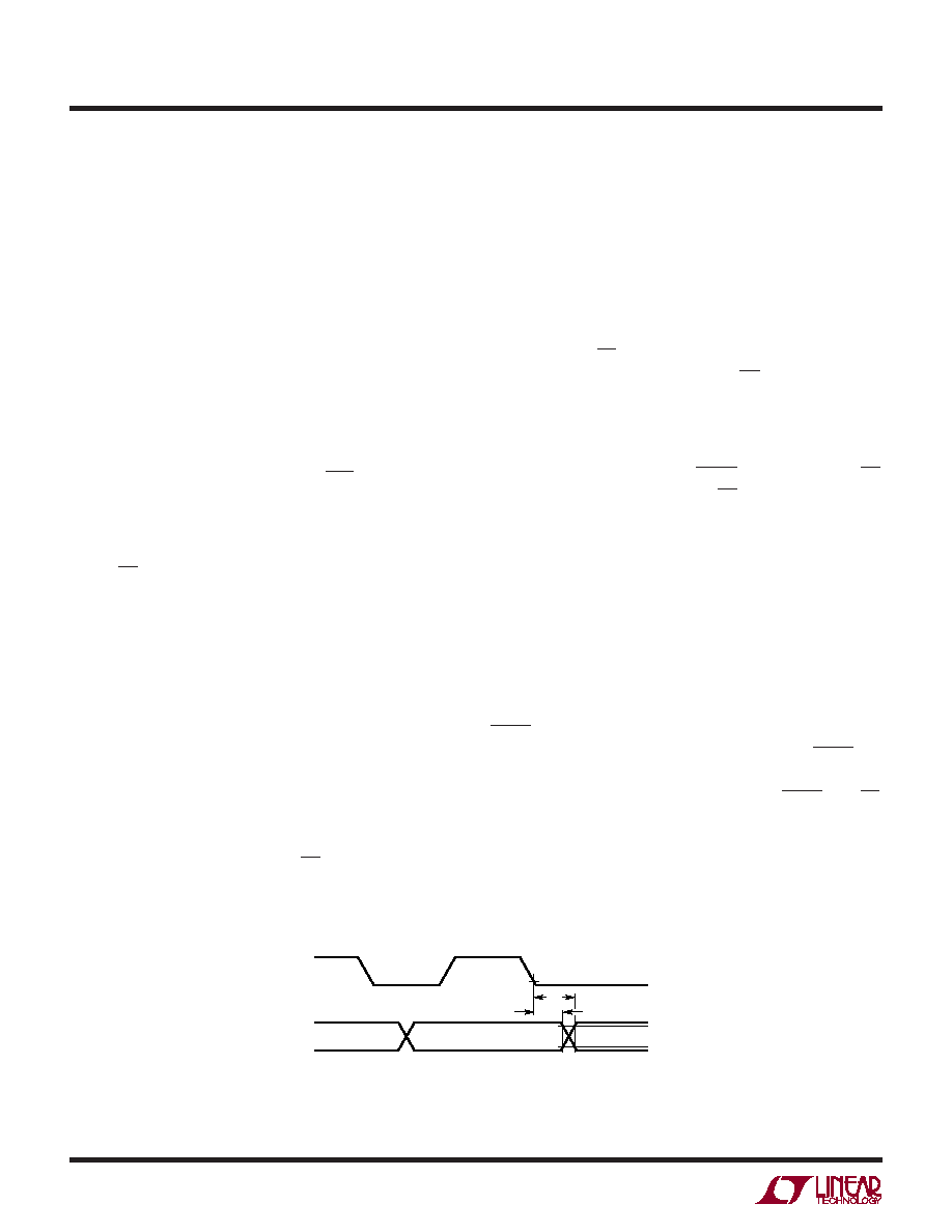
Figure 16. SCLK to DOUT Delay
t12
t11
SCLK
VIL
VOH
VOL
DOUT
1417 F16
相关PDF资料 |
PDF描述 |
|---|---|
| MS3102A22-28P | CONN RCPT 7POS BOX MNT W/PINS |
| VE-J3M-MY-F3 | CONVERTER MOD DC/DC 10V 50W |
| VE-J3L-MY-F2 | CONVERTER MOD DC/DC 28V 50W |
| MS3102C20-8P | CONN RCPT 6POS BOX MNT W/PINS |
| UMK105CK010CW-F | CAP CER 1PF 50V C0K 0402 |
相关代理商/技术参数 |
参数描述 |
|---|---|
| LTC1417CGN | 功能描述:IC A/D CONV 14BIT SAMPLNG 16SSOP RoHS:否 类别:集成电路 (IC) >> 数据采集 - 模数转换器 系列:- 标准包装:1,000 系列:- 位数:16 采样率(每秒):45k 数据接口:串行 转换器数目:2 功率耗散(最大):315mW 电压电源:模拟和数字 工作温度:0°C ~ 70°C 安装类型:表面贴装 封装/外壳:28-SOIC(0.295",7.50mm 宽) 供应商设备封装:28-SOIC W 包装:带卷 (TR) 输入数目和类型:2 个单端,单极 |
| LTC1417CGN#PBF | 功能描述:IC A/D CONV 14BIT SAMPLNG 16SSOP RoHS:是 类别:集成电路 (IC) >> 数据采集 - 模数转换器 系列:- 标准包装:1 系列:microPOWER™ 位数:8 采样率(每秒):1M 数据接口:串行,SPI? 转换器数目:1 功率耗散(最大):- 电压电源:模拟和数字 工作温度:-40°C ~ 125°C 安装类型:表面贴装 封装/外壳:24-VFQFN 裸露焊盘 供应商设备封装:24-VQFN 裸露焊盘(4x4) 包装:Digi-Reel® 输入数目和类型:8 个单端,单极 产品目录页面:892 (CN2011-ZH PDF) 其它名称:296-25851-6 |
| LTC1417CGN#PBF | 制造商:Linear Technology 功能描述:ADC, 14BIT, 400KSPS, SSOP-16 |
| LTC1417CGN#TR | 功能描述:IC ADC 14BIT 400KSPS SMPL 16SSOP RoHS:否 类别:集成电路 (IC) >> 数据采集 - 模数转换器 系列:- 标准包装:1,000 系列:- 位数:16 采样率(每秒):45k 数据接口:串行 转换器数目:2 功率耗散(最大):315mW 电压电源:模拟和数字 工作温度:0°C ~ 70°C 安装类型:表面贴装 封装/外壳:28-SOIC(0.295",7.50mm 宽) 供应商设备封装:28-SOIC W 包装:带卷 (TR) 输入数目和类型:2 个单端,单极 |
| LTC1417CGN#TRPBF | 功能描述:IC A/D CONV 14BIT SAMPLNG 16SSOP RoHS:是 类别:集成电路 (IC) >> 数据采集 - 模数转换器 系列:- 标准包装:1,000 系列:- 位数:16 采样率(每秒):45k 数据接口:串行 转换器数目:2 功率耗散(最大):315mW 电压电源:模拟和数字 工作温度:0°C ~ 70°C 安装类型:表面贴装 封装/外壳:28-SOIC(0.295",7.50mm 宽) 供应商设备封装:28-SOIC W 包装:带卷 (TR) 输入数目和类型:2 个单端,单极 |
发布紧急采购,3分钟左右您将得到回复。