- 您现在的位置:买卖IC网 > PDF目录10533 > LTC1417AIGN#PBF (Linear Technology)IC A/D CONV 14BIT SAMPLNG 16SSOP PDF资料下载
参数资料
| 型号: | LTC1417AIGN#PBF |
| 厂商: | Linear Technology |
| 文件页数: | 7/32页 |
| 文件大小: | 0K |
| 描述: | IC A/D CONV 14BIT SAMPLNG 16SSOP |
| 标准包装: | 100 |
| 位数: | 14 |
| 采样率(每秒): | 400k |
| 数据接口: | MICROWIRE?,串行,SPI? |
| 转换器数目: | 1 |
| 功率耗散(最大): | 27.5mW Unipolar; 44mW Bipolar |
| 电压电源: | 双 ± |
| 工作温度: | -40°C ~ 85°C |
| 安装类型: | 表面贴装 |
| 封装/外壳: | 16-SSOP(0.154",3.90mm 宽) |
| 供应商设备封装: | 16-SSOP |
| 包装: | 管件 |
| 输入数目和类型: | 2 个单端,单极;2 个单端,双极;1 个差分,单极;1 个差分,双极 |
第1页第2页第3页第4页第5页第6页当前第7页第8页第9页第10页第11页第12页第13页第14页第15页第16页第17页第18页第19页第20页第21页第22页第23页第24页第25页第26页第27页第28页第29页第30页第31页第32页
15
LTC1417
sn1417 1417fas
wait state during conversion or by using three-state buff-
ers to isolate the ADC data bus. The traces connecting the
pins and bypass capacitors must be kept short and should
be made as wide as possible.
The LTC1417 has differential inputs to minimize noise
coupling. Common mode noise on the AIN+ and AIN– leads
will be rejected by the input CMRR. The AIN– input can be
used as a ground sense for the AIN+ input; the LTC1417 will
hold and convert the difference voltage between AIN+ and
AIN–. The leads to AIN+ (Pin 1) and AIN– (Pin 2) should be
kept as short as possible. In applications where this is not
possible, the AIN+ and AIN– traces should be run side by
side to equalize coupling.
SUPPLY BYPASSING
High quality, low series resistance ceramic, 10
F bypass
capacitors should be used at the VDD and REFCOMP pins.
Surface mount ceramic capacitors such as Taiyo Yuden
LMK325BJ106MN provide excellent bypassing in a small
board space. Alternatively 10
F tantalum capacitors in
parallel with 0.1
F ceramic capacitors can be used.
Bypass capacitors must be located as close to the pins as
possible. The traces connecting the pins and the bypass
capacitors must be kept short and should be made as wide
as possible.
APPLICATIONS INFORMATION
WU
U
Example Layout
Figures 13a, 13b, 13c and 13d show the schematic and
layout of a suggested evaluation board. The layout demon-
strates the proper use of decoupling capacitors and ground
plane with a 2-layer printed circuit board.
POWER SHUTDOWN
The LTC1417 provides two power shutdown modes, Nap
and Sleep, to save power during inactive periods. The
Nap mode reduces ADC power dissipation by 80% and
leaves only the digital logic and reference powered up.
The wake-up time from Nap to active is 500ns (see Figure
14). In Sleep mode, all bias currents are shut down and
only leakage current remains— about 2
A. Wake-up
time from Sleep mode is much slower since the reference
circuit must power up and settle to 0.005% for full 14-bit
accuracy. Sleep mode wake-up time is dependent on the
value of the capacitor connected to the REFCOMP (Pin 4).
The wake-up time is 30ms with the recommended 10
F
capacitor. Shutdown is controlled by Pin 11 (SHDN); the
ADC is in shutdown when it is low. The shutdown mode
is selected with Pin 12 (RD); low selects Nap mode, high
selects Sleep mode.
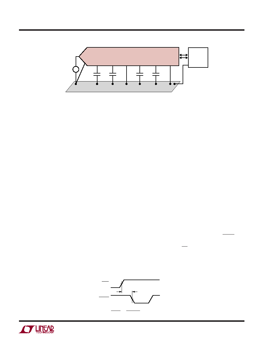
Figure 12. Power Supply Grounding Practice
1417 F12
DIGITAL
SYSTEM
ANALOG
INPUT
CIRCUITRY
5
4
2
15
16
10
1
10
F
3
1
F10F
10
F
ANALOG GROUND PLANE
+
–
AIN
+
AGND
REFCOMP
VSS
VREF
VDD
LTC1417
DGND
AIN
–
Figure 14. SHDN to CONVST Wake-Up Timing
t1
SHDN
CONVST
1417 F14
相关PDF资料 |
PDF描述 |
|---|---|
| MS3102A22-28P | CONN RCPT 7POS BOX MNT W/PINS |
| VE-J3M-MY-F3 | CONVERTER MOD DC/DC 10V 50W |
| VE-J3L-MY-F2 | CONVERTER MOD DC/DC 28V 50W |
| MS3102C20-8P | CONN RCPT 6POS BOX MNT W/PINS |
| UMK105CK010CW-F | CAP CER 1PF 50V C0K 0402 |
相关代理商/技术参数 |
参数描述 |
|---|---|
| LTC1417CGN | 功能描述:IC A/D CONV 14BIT SAMPLNG 16SSOP RoHS:否 类别:集成电路 (IC) >> 数据采集 - 模数转换器 系列:- 标准包装:1,000 系列:- 位数:16 采样率(每秒):45k 数据接口:串行 转换器数目:2 功率耗散(最大):315mW 电压电源:模拟和数字 工作温度:0°C ~ 70°C 安装类型:表面贴装 封装/外壳:28-SOIC(0.295",7.50mm 宽) 供应商设备封装:28-SOIC W 包装:带卷 (TR) 输入数目和类型:2 个单端,单极 |
| LTC1417CGN#PBF | 功能描述:IC A/D CONV 14BIT SAMPLNG 16SSOP RoHS:是 类别:集成电路 (IC) >> 数据采集 - 模数转换器 系列:- 标准包装:1 系列:microPOWER™ 位数:8 采样率(每秒):1M 数据接口:串行,SPI? 转换器数目:1 功率耗散(最大):- 电压电源:模拟和数字 工作温度:-40°C ~ 125°C 安装类型:表面贴装 封装/外壳:24-VFQFN 裸露焊盘 供应商设备封装:24-VQFN 裸露焊盘(4x4) 包装:Digi-Reel® 输入数目和类型:8 个单端,单极 产品目录页面:892 (CN2011-ZH PDF) 其它名称:296-25851-6 |
| LTC1417CGN#PBF | 制造商:Linear Technology 功能描述:ADC, 14BIT, 400KSPS, SSOP-16 |
| LTC1417CGN#TR | 功能描述:IC ADC 14BIT 400KSPS SMPL 16SSOP RoHS:否 类别:集成电路 (IC) >> 数据采集 - 模数转换器 系列:- 标准包装:1,000 系列:- 位数:16 采样率(每秒):45k 数据接口:串行 转换器数目:2 功率耗散(最大):315mW 电压电源:模拟和数字 工作温度:0°C ~ 70°C 安装类型:表面贴装 封装/外壳:28-SOIC(0.295",7.50mm 宽) 供应商设备封装:28-SOIC W 包装:带卷 (TR) 输入数目和类型:2 个单端,单极 |
| LTC1417CGN#TRPBF | 功能描述:IC A/D CONV 14BIT SAMPLNG 16SSOP RoHS:是 类别:集成电路 (IC) >> 数据采集 - 模数转换器 系列:- 标准包装:1,000 系列:- 位数:16 采样率(每秒):45k 数据接口:串行 转换器数目:2 功率耗散(最大):315mW 电压电源:模拟和数字 工作温度:0°C ~ 70°C 安装类型:表面贴装 封装/外壳:28-SOIC(0.295",7.50mm 宽) 供应商设备封装:28-SOIC W 包装:带卷 (TR) 输入数目和类型:2 个单端,单极 |
发布紧急采购,3分钟左右您将得到回复。