- 您现在的位置:买卖IC网 > PDF目录10533 > LTC1417AIGN#PBF (Linear Technology)IC A/D CONV 14BIT SAMPLNG 16SSOP PDF资料下载
参数资料
| 型号: | LTC1417AIGN#PBF |
| 厂商: | Linear Technology |
| 文件页数: | 6/32页 |
| 文件大小: | 0K |
| 描述: | IC A/D CONV 14BIT SAMPLNG 16SSOP |
| 标准包装: | 100 |
| 位数: | 14 |
| 采样率(每秒): | 400k |
| 数据接口: | MICROWIRE?,串行,SPI? |
| 转换器数目: | 1 |
| 功率耗散(最大): | 27.5mW Unipolar; 44mW Bipolar |
| 电压电源: | 双 ± |
| 工作温度: | -40°C ~ 85°C |
| 安装类型: | 表面贴装 |
| 封装/外壳: | 16-SSOP(0.154",3.90mm 宽) |
| 供应商设备封装: | 16-SSOP |
| 包装: | 管件 |
| 输入数目和类型: | 2 个单端,单极;2 个单端,双极;1 个差分,单极;1 个差分,双极 |
第1页第2页第3页第4页第5页当前第6页第7页第8页第9页第10页第11页第12页第13页第14页第15页第16页第17页第18页第19页第20页第21页第22页第23页第24页第25页第26页第27页第28页第29页第30页第31页第32页
14
LTC1417
sn1417 1417fas
APPLICATIONS INFORMATION
WU
U
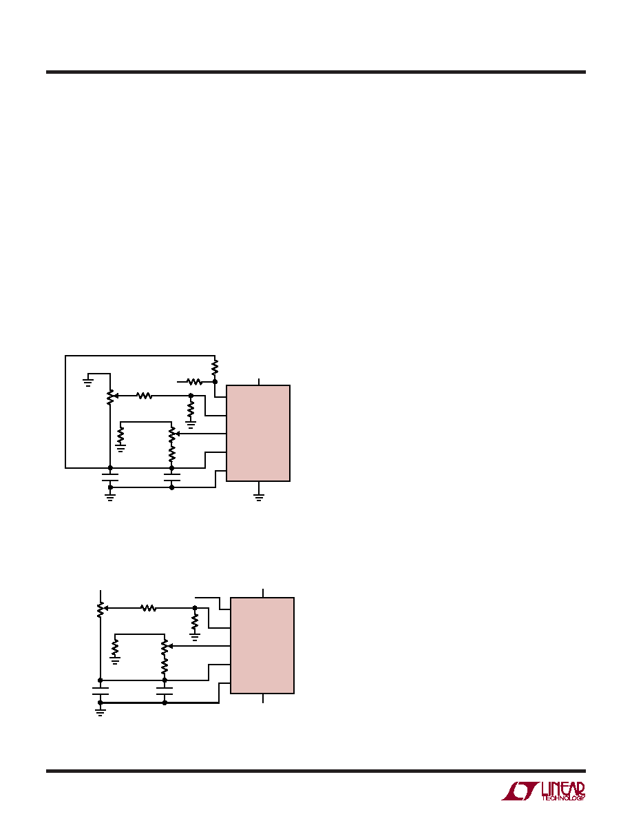
Figure 11b. Offset and Full-Scale Adjust Circuit
If – 5V Is Available
Figure 11a. Offset and Full-Scale Adjust Circuit
If – 5V Is Not Available
R2
50k
ANALOG INPUT
1417 F11a
5V
R4
100
R3
24k
R7
48k
R6
24k
R1
50k
R5
47k
0.1
F
10
F
R8
100
1
2
3
4
5
LTC1417
AIN
+
AIN
–
VREF
REFCOMP
AGND V
SS
VDD
OFFSET
ADJ
FS
ADJ
ANALOG INPUT
1417 F11b
5V
–5V
R4
100
R2
50k
FS
ADJ
OFFSET
ADJ
R3
24k
R6
24k
R1
50k
R5
47k
0.1
F
10
F
1
2
3
4
5
LTC1417
AIN
+
AIN
–
VREF
REFCOMP
AGND V
SS
VDD
Unipolar Offset and Full-Scale Error Adjustment
In applications where absolute accuracy is important,
offset and full-scale errors can be adjusted to zero. Offset
error must be adjusted before full-scale error. Figures
11a and 11b show the extra components required for full-
scale error adjustment. Zero offset is achieved by adjust-
ing the offset applied to the AIN– input. For zero offset
error, apply 125
V (i.e., 0.5LSB) at the input and adjust
the offset at the AIN– input until the output code flickers
between 0000 0000 0000 00 and 0000 0000 0000 01. For
full-scale adjustment, an input voltage of 4.095625V
(FS – 1.5LSBs) is applied to AIN+ and R2 is adjusted until
the output code flickers between 1111 1111 1111 10 and
1111 1111 1111 11.
Bipolar Offset and Full-Scale Error Adjustment
Bipolar offset and full-scale errors are adjusted in a
similar fashion to the unipolar case using the circuit in
Figure 11b. Again, bipolar offset error must be adjusted
before full-scale error. Bipolar offset error adjustment is
achieved by adjusting the offset applied to the AIN– input.
For zero offset error, apply – 125
V (i.e., –0.5LSB) at AIN+
and adjust the offset at the AIN– input until the output code
flickers between 0000 0000 0000 00 and 1111 1111 1111
11. For full-scale adjustment, an input voltage of 2.047625V
(FS – 1.5LSBs) is applied to AIN+ and R2 is adjusted until
the output code flickers between 0111 1111 1111 10 and
0111 1111 1111 11.
BOARD LAYOUT AND GROUNDING
To obtain the best performance from the LTC1417, a
printed circuit board with ground plane is required. The
ground plane under the ADC area should be as free of
breaks and holes as possible, such that a low impedance
path between all ADC grounds and all ADC decoupling
capacitors is provided. It is critical to prevent digital noise
from being coupled to the analog input, reference or
analog power supply lines. Layout should ensure that
digital and analog signal lines are separated as much as
possible. In particular, care should be taken not to run any
digital track alongside an analog signal track.
An analog ground plane separate from the logic system
ground should be established under and around the ADC.
Pin 5 (AGND) and Pin 10 (DGND) and all other analog
grounds should be connected to this single analog ground
plane. The REFCOMP bypass capacitor and the VDD by-
pass capacitor should also be connected to this analog
ground plane. No other digital grounds should be con-
nected to this analog ground plane. Low impedance ana-
log and digital power supply common returns are essential
to low noise operation of the ADC and the foil width for
these tracks should be as wide as possible. In applications
where the ADC data outputs and control signals are
connected to a continuously active microprocessor bus, it
is possible to get errors in the conversion results. These
errors are due to feedthrough from the microprocessor to
the successive approximation comparator. The problem
can be eliminated by forcing the microprocessor into a
相关PDF资料 |
PDF描述 |
|---|---|
| MS3102A22-28P | CONN RCPT 7POS BOX MNT W/PINS |
| VE-J3M-MY-F3 | CONVERTER MOD DC/DC 10V 50W |
| VE-J3L-MY-F2 | CONVERTER MOD DC/DC 28V 50W |
| MS3102C20-8P | CONN RCPT 6POS BOX MNT W/PINS |
| UMK105CK010CW-F | CAP CER 1PF 50V C0K 0402 |
相关代理商/技术参数 |
参数描述 |
|---|---|
| LTC1417CGN | 功能描述:IC A/D CONV 14BIT SAMPLNG 16SSOP RoHS:否 类别:集成电路 (IC) >> 数据采集 - 模数转换器 系列:- 标准包装:1,000 系列:- 位数:16 采样率(每秒):45k 数据接口:串行 转换器数目:2 功率耗散(最大):315mW 电压电源:模拟和数字 工作温度:0°C ~ 70°C 安装类型:表面贴装 封装/外壳:28-SOIC(0.295",7.50mm 宽) 供应商设备封装:28-SOIC W 包装:带卷 (TR) 输入数目和类型:2 个单端,单极 |
| LTC1417CGN#PBF | 功能描述:IC A/D CONV 14BIT SAMPLNG 16SSOP RoHS:是 类别:集成电路 (IC) >> 数据采集 - 模数转换器 系列:- 标准包装:1 系列:microPOWER™ 位数:8 采样率(每秒):1M 数据接口:串行,SPI? 转换器数目:1 功率耗散(最大):- 电压电源:模拟和数字 工作温度:-40°C ~ 125°C 安装类型:表面贴装 封装/外壳:24-VFQFN 裸露焊盘 供应商设备封装:24-VQFN 裸露焊盘(4x4) 包装:Digi-Reel® 输入数目和类型:8 个单端,单极 产品目录页面:892 (CN2011-ZH PDF) 其它名称:296-25851-6 |
| LTC1417CGN#PBF | 制造商:Linear Technology 功能描述:ADC, 14BIT, 400KSPS, SSOP-16 |
| LTC1417CGN#TR | 功能描述:IC ADC 14BIT 400KSPS SMPL 16SSOP RoHS:否 类别:集成电路 (IC) >> 数据采集 - 模数转换器 系列:- 标准包装:1,000 系列:- 位数:16 采样率(每秒):45k 数据接口:串行 转换器数目:2 功率耗散(最大):315mW 电压电源:模拟和数字 工作温度:0°C ~ 70°C 安装类型:表面贴装 封装/外壳:28-SOIC(0.295",7.50mm 宽) 供应商设备封装:28-SOIC W 包装:带卷 (TR) 输入数目和类型:2 个单端,单极 |
| LTC1417CGN#TRPBF | 功能描述:IC A/D CONV 14BIT SAMPLNG 16SSOP RoHS:是 类别:集成电路 (IC) >> 数据采集 - 模数转换器 系列:- 标准包装:1,000 系列:- 位数:16 采样率(每秒):45k 数据接口:串行 转换器数目:2 功率耗散(最大):315mW 电压电源:模拟和数字 工作温度:0°C ~ 70°C 安装类型:表面贴装 封装/外壳:28-SOIC(0.295",7.50mm 宽) 供应商设备封装:28-SOIC W 包装:带卷 (TR) 输入数目和类型:2 个单端,单极 |
发布紧急采购,3分钟左右您将得到回复。