- 您现在的位置:买卖IC网 > PDF目录44988 > LTC1628IG-SYNC#TR (LINEAR TECHNOLOGY CORP) 3 A SWITCHING CONTROLLER, 360 kHz SWITCHING FREQ-MAX, PDSO28 PDF资料下载
参数资料
| 型号: | LTC1628IG-SYNC#TR |
| 厂商: | LINEAR TECHNOLOGY CORP |
| 元件分类: | 稳压器 |
| 英文描述: | 3 A SWITCHING CONTROLLER, 360 kHz SWITCHING FREQ-MAX, PDSO28 |
| 封装: | 0.209 INCH, PLASTIC, SSOP-28 |
| 文件页数: | 10/32页 |
| 文件大小: | 658K |
| 代理商: | LTC1628IG-SYNC#TR |
第1页第2页第3页第4页第5页第6页第7页第8页第9页当前第10页第11页第12页第13页第14页第15页第16页第17页第18页第19页第20页第21页第22页第23页第24页第25页第26页第27页第28页第29页第30页第31页第32页
18
LTC1628-SYNC
1628syncfa
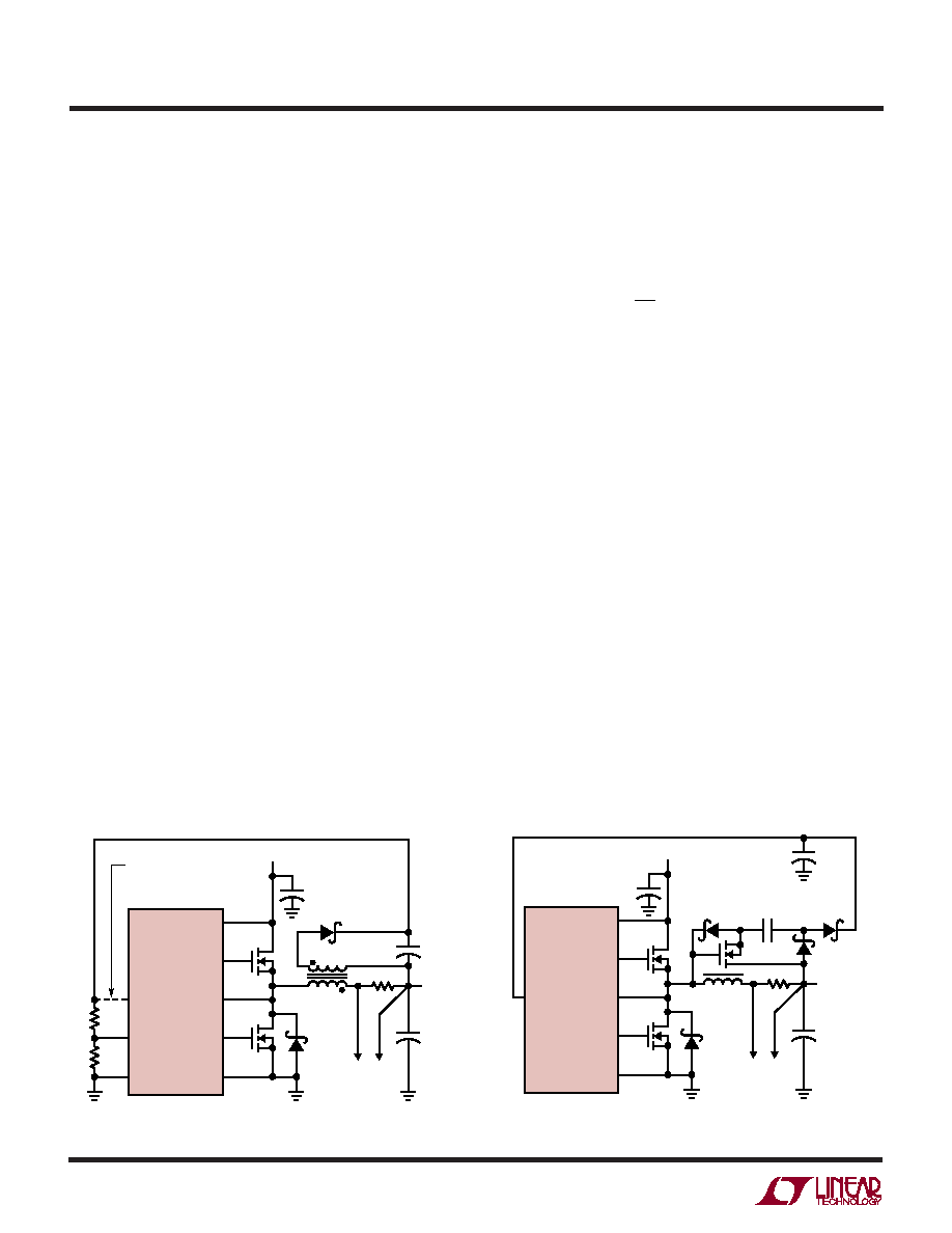
output-derived voltage that has been boosted to greater
than 4.7V. This can be done with either the inductive boost
winding as shown in Figure 6a or the capacitive charge
pump shown in Figure 6b. The charge pump has the
advantage of simple magnetics.
Topside MOSFET Driver Supply (CB, DB)
External bootstrap capacitors CB connected to the BOOST
pins supply the gate drive voltages for the topside MOS-
FETs. Capacitor CB in the functional diagram is charged
though external diode DB from INTVCC when the SW pin is
low. When one of the topside MOSFETs is to be turned on,
the driver places the CB voltage across the gate-source of
the desired MOSFET. This enhances the MOSFET and
turns on the topside switch. The switch node voltage, SW,
rises to VIN and the BOOST pin follows. With the topside
MOSFET on, the boost voltage is above the input supply:
VBOOST = VIN + VINTVCC. The value of the boost capacitor
CB needs to be 100 times that of the total input capacitance
of the topside MOSFET(s). The reverse breakdown of the
external Schottky diode must be greater than VIN(MAX).
When adjusting the gate drive level, the final arbiter is the
total input current for the regulator. If a change is made
and the input current decreases, then the efficiency has
improved. If there is no change in input current, then there
is no change in efficiency.
Output Voltage
The LTC1628-SYNC output voltages are each set by an
external feedback resistive divider carefully placed across
Figure 6a. Secondary Output Loop & EXTVCC Connection
Figure 6b. Capacitive Charge Pump for EXTVCC
the output capacitor. The resultant feedback signal is
compared with the internal precision 0.800V voltage ref-
erence by the error amplifier. The output voltage is given
by the equation:
VV
R
OUT =+
08
1
2
1
.
where R1 and R2 are defined in Figure 2.
SENSE+/SENSE– Pins
The common mode input range of the current comparator
sense pins is from 0V to (1.1)INTVCC. Continuous linear
operation is guaranteed throughout this range allowing
output voltage setting from 0.8V to 7.7V, depending upon
the voltage applied to EXTVCC. A differential NPN input
stage is biased with internal resistors from an internal
2.4V source as shown in the Functional Diagram. This
requires that current either be sourced or sunk from the
SENSE pins depending on the output voltage. If the output
voltage is below 2.4V current will flow out of both SENSE
pins to the main output. The output can be easily preloaded
by the VOUT resistive divider to compensate for the current
comparator’s negative input bias current. The maximum
current flowing out of each pair of SENSE pins is:
ISENSE+ + ISENSE– = (2.4V – VOUT)/24k
Since VOSENSE is servoed to the 0.8V reference voltage, we
can choose R1 in Figure 2 to have a maximum value to
absorb this current.
EXTVCC
FCB
SGND
VIN
TG1
SW
BG1
PGND
LTC1628-SYNC
RSENSE
VOUT
VSEC
+
COUT
+
1
F
1628 F06a
N-CH
R6
+
CIN
VIN
T1
1:N
OPTIONAL EXTVCC
CONNECTION
5V < VSEC < 7V
R5
EXTVCC
VIN
TG1
SW
BG1
PGND
LTC1628-SYNC
RSENSE
VOUT
VN2222LL
+
COUT
1628 F06b
N-CH
+
CIN
+
1
F
VIN
L1
BAT85
0.22
F
APPLICATIO S I FOR ATIO
WU
UU
相关PDF资料 |
PDF描述 |
|---|---|
| LTC1643HCGN#PBF | 4-CHANNEL POWER SUPPLY SUPPORT CKT, PDSO16 |
| LTC1643LCGN#TR | 4-CHANNEL POWER SUPPLY SUPPORT CKT, PDSO16 |
| LTC1728HS5-5 | 3-CHANNEL POWER SUPPLY SUPPORT CKT, PDSO5 |
| LTC1729CS8-8.4#TR | 1-CHANNEL POWER SUPPLY SUPPORT CKT, PDSO8 |
| LTC1772BIS6#PBF | 1 A SWITCHING CONTROLLER, 650 kHz SWITCHING FREQ-MAX, PDSO6 |
相关代理商/技术参数 |
参数描述 |
|---|---|
| LTC1628IUH | 功能描述:IC REG CTRLR BUCK PWM CM 32-QFN RoHS:否 类别:集成电路 (IC) >> PMIC - 稳压器 - DC DC 切换控制器 系列:- 标准包装:4,500 系列:PowerWise® PWM 型:控制器 输出数:1 频率 - 最大:1MHz 占空比:95% 电源电压:2.8 V ~ 5.5 V 降压:是 升压:无 回扫:无 反相:无 倍增器:无 除法器:无 Cuk:无 隔离:无 工作温度:-40°C ~ 125°C 封装/外壳:6-WDFN 裸露焊盘 包装:带卷 (TR) 配用:LM1771EVAL-ND - BOARD EVALUATION LM1771 其它名称:LM1771SSDX |
| LTC1628IUH#PBF | 功能描述:IC REG CTRLR BUCK PWM CM 32-QFN RoHS:是 类别:集成电路 (IC) >> PMIC - 稳压器 - DC DC 切换控制器 系列:- 标准包装:4,500 系列:PowerWise® PWM 型:控制器 输出数:1 频率 - 最大:1MHz 占空比:95% 电源电压:2.8 V ~ 5.5 V 降压:是 升压:无 回扫:无 反相:无 倍增器:无 除法器:无 Cuk:无 隔离:无 工作温度:-40°C ~ 125°C 封装/外壳:6-WDFN 裸露焊盘 包装:带卷 (TR) 配用:LM1771EVAL-ND - BOARD EVALUATION LM1771 其它名称:LM1771SSDX |
| LTC1628IUH#TR | 功能描述:IC REG CTRLR BUCK PWM CM 32-QFN RoHS:否 类别:集成电路 (IC) >> PMIC - 稳压器 - DC DC 切换控制器 系列:- 标准包装:4,500 系列:PowerWise® PWM 型:控制器 输出数:1 频率 - 最大:1MHz 占空比:95% 电源电压:2.8 V ~ 5.5 V 降压:是 升压:无 回扫:无 反相:无 倍增器:无 除法器:无 Cuk:无 隔离:无 工作温度:-40°C ~ 125°C 封装/外壳:6-WDFN 裸露焊盘 包装:带卷 (TR) 配用:LM1771EVAL-ND - BOARD EVALUATION LM1771 其它名称:LM1771SSDX |
| LTC1628IUH#TRPBF | 功能描述:IC REG CTRLR BUCK PWM CM 32-QFN RoHS:是 类别:集成电路 (IC) >> PMIC - 稳压器 - DC DC 切换控制器 系列:- 标准包装:4,500 系列:PowerWise® PWM 型:控制器 输出数:1 频率 - 最大:1MHz 占空比:95% 电源电压:2.8 V ~ 5.5 V 降压:是 升压:无 回扫:无 反相:无 倍增器:无 除法器:无 Cuk:无 隔离:无 工作温度:-40°C ~ 125°C 封装/外壳:6-WDFN 裸露焊盘 包装:带卷 (TR) 配用:LM1771EVAL-ND - BOARD EVALUATION LM1771 其它名称:LM1771SSDX |
| LTC1629CG | 功能描述:IC REG CTRLR BUCK PWM CM 28-SSOP RoHS:否 类别:集成电路 (IC) >> PMIC - 稳压器 - DC DC 切换控制器 系列:PolyPhase® 标准包装:4,500 系列:PowerWise® PWM 型:控制器 输出数:1 频率 - 最大:1MHz 占空比:95% 电源电压:2.8 V ~ 5.5 V 降压:是 升压:无 回扫:无 反相:无 倍增器:无 除法器:无 Cuk:无 隔离:无 工作温度:-40°C ~ 125°C 封装/外壳:6-WDFN 裸露焊盘 包装:带卷 (TR) 配用:LM1771EVAL-ND - BOARD EVALUATION LM1771 其它名称:LM1771SSDX |
发布紧急采购,3分钟左右您将得到回复。