- 您现在的位置:买卖IC网 > PDF目录1827 > LTC1649CS#PBF (Linear Technology)IC REG CTRLR BUCK PWM VM 16-SOIC PDF资料下载
参数资料
| 型号: | LTC1649CS#PBF |
| 厂商: | Linear Technology |
| 文件页数: | 11/16页 |
| 文件大小: | 0K |
| 描述: | IC REG CTRLR BUCK PWM VM 16-SOIC |
| 标准包装: | 50 |
| PWM 型: | 电压模式 |
| 输出数: | 1 |
| 频率 - 最大: | 260kHz |
| 占空比: | 93% |
| 电源电压: | 2.7 V ~ 5 V |
| 降压: | 是 |
| 升压: | 无 |
| 回扫: | 无 |
| 反相: | 无 |
| 倍增器: | 无 |
| 除法器: | 无 |
| Cuk: | 无 |
| 隔离: | 无 |
| 工作温度: | 0°C ~ 70°C |
| 封装/外壳: | 16-SOIC(0.154",3.90mm 宽) |
| 包装: | 管件 |
�� �
�
�LTC1649�
�APPLICATIO� N� S� I� N� FOR� M� ATIO� N�
�The� CP� OUT� pin� can� typically� supply� 50mA� at� 5V,� adequate�
�to� power� the� V� CC� and� PV� CC� pins.� This� supply� can� also� be�
�used� to� power� external� circuitry,� but� any� additional� current�
�drawn� from� CP� OUT� subtracts� from� the� current� available� to�
�drive� the� external� MOSFETs.� Circuits� with� small� external�
�MOSFETs� can� draw� as� much� as� 20mA� or� 30mA� from�
�CP� OUT� without� hindering� performance.� High� output� cur-�
�rent� circuits� with� large� or� multiple� external� MOSFETs� may�
�need� every� milliamp� they� can� get� from� CP� OUT� ,� and� external�
�loads� should� be� minimized.� The� charge� pump� at� PV� CC1� is�
�more� limited� in� its� abilities,� and� should� not� be� connected�
�to� anything� except� PV� CC1� .� In� particular,� do� not� connect� a�
�bypass� capacitor� from� PV� CC1� to� ground—it� will� steal�
�charge� from� the� charge� pump� and� actually� degrade� perfor-�
�Output� transient� response� is� set� by� three� major� factors:� the�
�time� constant� of� the� inductor� and� the� output� capacitor,� the�
�ESR� of� the� output� capacitor,� and� the� loop� compensation�
�components.� The� first� two� factors� usually� have� much�
�more� impact� on� overall� transient� recovery� time� than� the�
�third;� unless� the� loop� compensation� is� way� off,� more�
�improvement� can� be� had� by� optimizing� the� inductor� and�
�the� output� capacitor� than� by� fiddling� with� the� loop� com-�
�pensation� components.� In� general,� a� smaller� value� induc-�
�tor� will� improve� transient� response� at� the� expense� of� ripple�
�and� inductor� core� saturation� rating.� Minimizing� output�
�capacitor� ESR� will� also� help� optimize� output� transient�
�response.� See� Input� and� Output� Capacitors� for� more�
�information.�
�mance.�
�Soft� Start� and� Current� Limit�
�Compensation� and� Transient� Response�
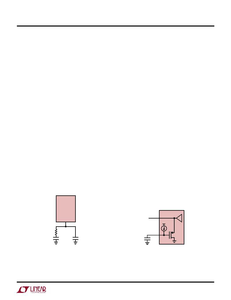
�The� LTC1649� voltage� feedback� loop� is� compensated� at� the�
�COMP� pin;� this� is� the� output� node� of� the� internal� g� m� error�
�amplifier.� The� loop� can� generally� be� compensated� prop-�
�erly� with� an� RC� network� from� COMP� to� GND� and� an�
�additional� small� C� from� COMP� to� GND� (Figure� 5).� Loop�
�stability� is� affected� by� inductor� and� output� capacitor�
�values� and� by� other� factors.� Optimum� loop� response� can�
�be� obtained� by� using� a� network� analyzer� to� find� the� loop�
�poles� and� zeros;� nearly� as� effective� and� a� lot� easier� is� to�
�empirically� tweak� the� R� C� values� until� the� transient� recovery�
�looks� right� with� an� output� load� step.�
�The� LTC1649� includes� a� soft� start� circuit� at� the� SS� pin;� this�
�circuit� is� used� both� for� initial� start-up� and� during� current�
�limit� operation.� SS� requires� an� external� capacitor� to� GND�
�with� the� value� determined� by� the� required� soft� start� time.�
�An� internal� 12� μ� A� current� source� is� included� to� charge� the�
�external� capacitor.� Soft� start� functions� by� clamping� the�
�maximum� voltage� that� the� COMP� pin� can� swing� to,� thereby�
�controlling� the� duty� cycle� (Figure� 6).� The� LTC1649� will�
�begin� to� operate� at� low� duty� cycle� as� the� SS� pin� rises� to�
�about� 2V� below� the� V� CC� pin.� As� SS� continues� to� rise,� the�
�duty� cycle� will� increase� until� the� error� amplifier� takes� over�
�and� begins� to� regulate� the� output.� When� SS� reaches� 1V�
�below� V� CC� the� LTC1649� will� be� in� full� operation.� An� internal�
�switch� shorts� the� SS� pin� to� GND� during� shutdown.�
�LTC1649�
�COMP�
�COMP�
�V� CC�
�LTC1649�
�FB�
�12� μ� A�
�R� C�
�SS�
�C� C�
�C1�
�C� SS�
�1659� F05�
�Figure� 5.� Compensation� Pin� Hook-Up�
�1649� F06�
�Figure� 6.� Soft� Start� Clamps� COMP� Pin�
�11�
�相关PDF资料 |
PDF描述 |
|---|---|
| LTC1682CS8-5 | IC REG MULTI CONFIG 5V 8SOIC |
| LTC1697EMS#TRPBF | IC REG SW 1W CCFL LOW PWR 10MSOP |
| LTC1698EGN | IC REG CTRLR ISO PWM CM 16-SSOP |
| LTC1700EMS#PBF | IC REG CTRLR BST PWM CM 10-MSOP |
| LTC1701BES5#TRMPBF | IC REG BUCK ADJ 0.5A TSOT23-5 |
相关代理商/技术参数 |
参数描述 |
|---|---|
| LTC1649IS | 功能描述:IC REG CTRLR BUCK PWM VM 16-SOIC RoHS:否 类别:集成电路 (IC) >> PMIC - 稳压器 - DC DC 切换控制器 系列:- 标准包装:4,500 系列:PowerWise® PWM 型:控制器 输出数:1 频率 - 最大:1MHz 占空比:95% 电源电压:2.8 V ~ 5.5 V 降压:是 升压:无 回扫:无 反相:无 倍增器:无 除法器:无 Cuk:无 隔离:无 工作温度:-40°C ~ 125°C 封装/外壳:6-WDFN 裸露焊盘 包装:带卷 (TR) 配用:LM1771EVAL-ND - BOARD EVALUATION LM1771 其它名称:LM1771SSDX |
| LTC1649IS#PBF | 功能描述:IC REG CTRLR BUCK PWM VM 16-SOIC RoHS:是 类别:集成电路 (IC) >> PMIC - 稳压器 - DC DC 切换控制器 系列:- 标准包装:4,500 系列:PowerWise® PWM 型:控制器 输出数:1 频率 - 最大:1MHz 占空比:95% 电源电压:2.8 V ~ 5.5 V 降压:是 升压:无 回扫:无 反相:无 倍增器:无 除法器:无 Cuk:无 隔离:无 工作温度:-40°C ~ 125°C 封装/外壳:6-WDFN 裸露焊盘 包装:带卷 (TR) 配用:LM1771EVAL-ND - BOARD EVALUATION LM1771 其它名称:LM1771SSDX |
| LTC1649IS#TR | 功能描述:IC REG CTRLR BUCK PWM VM 16-SOIC RoHS:否 类别:集成电路 (IC) >> PMIC - 稳压器 - DC DC 切换控制器 系列:- 标准包装:4,500 系列:PowerWise® PWM 型:控制器 输出数:1 频率 - 最大:1MHz 占空比:95% 电源电压:2.8 V ~ 5.5 V 降压:是 升压:无 回扫:无 反相:无 倍增器:无 除法器:无 Cuk:无 隔离:无 工作温度:-40°C ~ 125°C 封装/外壳:6-WDFN 裸露焊盘 包装:带卷 (TR) 配用:LM1771EVAL-ND - BOARD EVALUATION LM1771 其它名称:LM1771SSDX |
| LTC1649IS#TRPBF | 功能描述:IC REG CTRLR BUCK PWM VM 16-SOIC RoHS:是 类别:集成电路 (IC) >> PMIC - 稳压器 - DC DC 切换控制器 系列:- 标准包装:4,500 系列:PowerWise® PWM 型:控制器 输出数:1 频率 - 最大:1MHz 占空比:95% 电源电压:2.8 V ~ 5.5 V 降压:是 升压:无 回扫:无 反相:无 倍增器:无 除法器:无 Cuk:无 隔离:无 工作温度:-40°C ~ 125°C 封装/外壳:6-WDFN 裸露焊盘 包装:带卷 (TR) 配用:LM1771EVAL-ND - BOARD EVALUATION LM1771 其它名称:LM1771SSDX |
| LTC1650ACN | 功能描述:IC D/A CONV 16BIT R-R 16-DIP RoHS:否 类别:集成电路 (IC) >> 数据采集 - 数模转换器 系列:- 产品培训模块:Data Converter Fundamentals DAC Architectures 标准包装:750 系列:- 设置时间:7µs 位数:16 数据接口:并联 转换器数目:1 电压电源:双 ± 功率耗散(最大):100mW 工作温度:0°C ~ 70°C 安装类型:表面贴装 封装/外壳:28-LCC(J 形引线) 供应商设备封装:28-PLCC(11.51x11.51) 包装:带卷 (TR) 输出数目和类型:1 电压,单极;1 电压,双极 采样率(每秒):143k |
发布紧急采购,3分钟左右您将得到回复。