- 您现在的位置:买卖IC网 > PDF目录1827 > LTC1703IG#TRPBF (Linear Technology)IC REG SW DUAL SYNC VID 28SSOP PDF资料下载
参数资料
| 型号: | LTC1703IG#TRPBF |
| 厂商: | Linear Technology |
| 文件页数: | 25/36页 |
| 文件大小: | 0K |
| 描述: | IC REG SW DUAL SYNC VID 28SSOP |
| 标准包装: | 2,000 |
| 应用: | 控制器,移动式 Intel Pentium? III |
| 输入电压: | 3 V ~ 7 V |
| 输出数: | 2 |
| 输出电压: | 0.9 V ~ 2 V |
| 工作温度: | -40°C ~ 85°C |
| 安装类型: | 表面贴装 |
| 封装/外壳: | 28-SSOP(0.209",5.30mm 宽) |
| 供应商设备封装: | 28-SSOP |
| 包装: | 带卷 (TR) |
第1页第2页第3页第4页第5页第6页第7页第8页第9页第10页第11页第12页第13页第14页第15页第16页第17页第18页第19页第20页第21页第22页第23页第24页当前第25页第26页第27页第28页第29页第30页第31页第32页第33页第34页第35页第36页
�� �
�
�LTC1703�
�APPLICATIO� S� I� FOR� ATIO�
�Accuracy� Trade-Offs�
�The� V� DS� sensing� scheme� used� in� the� LTC1703� is� not�
�particularly� accurate,� primarily� due� to� uncertainty� in� the�
�R� DS(ON)� from� MOSFET� to� MOSFET.� A� second� error� term�
�arises� from� the� ringing� present� at� the� SW� pin,� which�
�causes� the� V� DS� to� look� larger� than� (I� LOAD� )(R� DS(ON)� )� at� the�
�beginning� of� QB’s� on-time.� These� inaccuracies� do� not�
�prevent� the� LTC1703� current� limit� circuit� from� protecting�
�itself� and� the� load� from� damaging� overcurrent� conditions,�
�but� they� do� prevent� the� user� from� setting� the� current� limit�
�to� a� tight� tolerance� if� more� than� one� copy� of� the� circuit� is�
�being� built.� The� 50%� factor� in� the� current� setting� equation�
�above� reflects� the� margin� necessary� to� ensure� that� the�
�drops,� the� FCB� pin� will� trip� and� the� LTC1703� will� resume�
�continuous� operation� regardless� of� the� load� on� the� main�
�output.� The� FCB� pin� removes� the� requirement� that� power�
�must� be� drawn� from� the� inductor� primary� in� order� to�
�extract� power� from� the� auxiliary� windings.� With� the� loop� in�
�continuous� mode,� the� auxiliary� outputs� may� be� loaded�
�without� regard� to� the� primary� load.� Note� that� if� the� LTC1703�
�is� already� running� in� continuous� mode� and� the� auxiliary�
�output� drops� due� to� excessive� loading,� no� additional�
�action� can� be� taken� by� the� LTC1703� to� regulate� the�
�auxiliary� output.�
�V� IN�
�circuit� will� stay� out� of� current� limit� at� the� maximum� normal�
�load,� even� with� a� hot� MOSFET� that� is� running� quite� a� bit�
�higher� than� its� R� DS(ON)� spec.�
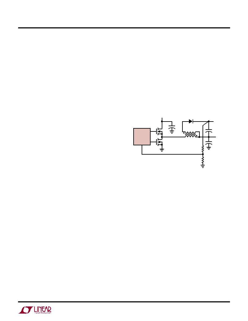
�FCB� OPERATION/SECONDARY� WINDINGS�
�TG�
�LTC1703�
�FCB� BG�
�QT�
�QB�
�+�
�C� IN�
�R� FCB1�
�+�
�+�
�V� OUT(AUX)�
�C� OUT(AUX)�
�V� OUT�
�C� OUT�
�The� FCB� pin� can� be� used� in� conjunction� with� a� secondary�
�winding� on� one� side� of� the� LTC1703� to� generate� a� third�
�regulated� voltage� output.� This� output� can� be� directly�
�regulated� at� the� FCB� pin.� In� theory,� a� fourth� output� could�
�be� added,� either� unregulated� or� with� additional� external�
�circuitry� at� the� FCB� pin.�
�The� extra� auxiliary� output� is� taken� from� a� second� winding�
�on� the� core� of� the� inductor� on� one� channel,� converting� it�
�into� a� transformer� (Figure� 13).� The� auxiliary� output� voltage�
�is� set� by� the� main� output� voltage� and� the� turns� ratio� of� the�
�extra� winding� to� the� primary� winding.� Load� regulation� at�
�the� auxiliary� output� will� be� relatively� good� as� long� as� the�
�main� output� is� running� in� continuous� mode.� As� the� load� on�
�the� main� channel� drops� and� the� LTC1703� switches� to�
�discontinuous� or� Burst� Mode� operation,� the� auxiliary�
�output� will� not� be� able� to� maintain� regulation,� especially� if�
�the� load� at� the� auxiliary� output� remains� heavy.�
�To� avoid� this,� the� auxiliary� output� voltage� is� divided� down�
�with� a� conventional� feedback� resistor� string� with� the�
�divided� auxiliary� output� voltage� fed� back� to� the� FCB� pin�
�(Figure� 13).� The� FCB� pin� threshold� is� trimmed� to� 800mV�
�with� 20mV� of� hysteresis,� allowing� fairly� precise� control� of�
�the� auxiliary� voltage.� If� the� LTC1703� is� in� discontinuous� or�
�Burst� Mode� operation� and� the� auxiliary� output� voltage�
�R� FCB2�
�1703� F13�
�Figure� 13.� Regulating� an� Auxiliary� Output� with� the� FCB� Pin�
�FAULT� FLAG�
�The� FAULT� pin� is� an� open-drain� output� that� indicates� if� one�
�or� both� of� the� outputs� has� exceeded� 15%� of� its� pro-�
�grammed� output� voltage.� FAULT� includes� an� internal�
�10� μ� A� pull-up� to� V� CC� and� does� not� require� an� external� pull-�
�up� to� interface� to� standard� logic.� FAULT� pulls� low� in�
�normal� operation,� and� releases� when� a� overvoltage� fault� is�
�detected.�
�When� an� overvoltage� fault� occurs,� an� internal� latch� sets�
�and� FAULT� goes� high,� disabling� the� LTC1703� until� the�
�latch� is� cleared� by� recycling� the� power� or� pulling� both�
�RUN/SS� pins� low� simultaneously.� Alternately,� the� FAULT�
�pin� can� be� pulled� back� low� externally� with� an� open-�
�collector/open-drain� device� or� an� N-channel� MOSFET� or�
�NPN,� which� will� allow� the� LTC1703� to� resume� normal�
�operation,� but� will� not� reset� the� latch.� If� the� pull-down� is�
�later� removed,� the� LTC1703� will� latch� off� again� unless� the�
�latch� is� reset� by� cycling� the� power� or� RUN/SS� pins.�
�1703fa�
�25�
�相关PDF资料 |
PDF描述 |
|---|---|
| LTC1707IS8#TRPBF | IC REG BUCK SYNC ADJ 0.6A 8SOIC |
| LTC1708EG-PG#TRPBF | IC REG CTRLR BUCK PWM CM 36-SSOP |
| LTC1709EG-7#TRPBF | IC REG CTRLR BUCK PWM CM 36-SSOP |
| LTC1709EG-8#TRPBF | IC REG CTRLR BUCK PWM CM 36-SSOP |
| LTC1709EG#PBF | IC REG CTRLR BUCK PWM CM 36-SSOP |
相关代理商/技术参数 |
参数描述 |
|---|---|
| LTC1704BEGN | 功能描述:IC REG DL BUCK/LINEAR 16-SSOP RoHS:否 类别:集成电路 (IC) >> PMIC - 稳压器 - 线性 + 切换式 系列:- 标准包装:2,500 系列:- 拓扑:降压(降压)同步(3),线性(LDO)(2) 功能:任何功能 输出数:5 频率 - 开关:300kHz 电压/电流 - 输出 1:控制器 电压/电流 - 输出 2:控制器 电压/电流 - 输出 3:控制器 带 LED 驱动器:无 带监控器:无 带序列发生器:是 电源电压:5.6 V ~ 24 V 工作温度:-40°C ~ 85°C 安装类型:* 封装/外壳:* 供应商设备封装:* 包装:* |
| LTC1704BEGN#PBF | 功能描述:IC REG DL BUCK/LINEAR 16-SSOP RoHS:是 类别:集成电路 (IC) >> PMIC - 稳压器 - 线性 + 切换式 系列:- 标准包装:2,500 系列:- 拓扑:降压(降压)同步(3),线性(LDO)(2) 功能:任何功能 输出数:5 频率 - 开关:300kHz 电压/电流 - 输出 1:控制器 电压/电流 - 输出 2:控制器 电压/电流 - 输出 3:控制器 带 LED 驱动器:无 带监控器:无 带序列发生器:是 电源电压:5.6 V ~ 24 V 工作温度:-40°C ~ 85°C 安装类型:* 封装/外壳:* 供应商设备封装:* 包装:* |
| LTC1704BEGN#TR | 功能描述:IC REG DL BUCK/LINEAR 16-SSOP RoHS:否 类别:集成电路 (IC) >> PMIC - 稳压器 - 线性 + 切换式 系列:- 标准包装:2,500 系列:- 拓扑:降压(降压)同步(3),线性(LDO)(2) 功能:任何功能 输出数:5 频率 - 开关:300kHz 电压/电流 - 输出 1:控制器 电压/电流 - 输出 2:控制器 电压/电流 - 输出 3:控制器 带 LED 驱动器:无 带监控器:无 带序列发生器:是 电源电压:5.6 V ~ 24 V 工作温度:-40°C ~ 85°C 安装类型:* 封装/外壳:* 供应商设备封装:* 包装:* |
| LTC1704BEGN#TRPBF | 功能描述:IC REG DL BUCK/LINEAR 16-SSOP RoHS:是 类别:集成电路 (IC) >> PMIC - 稳压器 - 线性 + 切换式 系列:- 标准包装:2,500 系列:- 拓扑:降压(降压)同步(3),线性(LDO)(2) 功能:任何功能 输出数:5 频率 - 开关:300kHz 电压/电流 - 输出 1:控制器 电压/电流 - 输出 2:控制器 电压/电流 - 输出 3:控制器 带 LED 驱动器:无 带监控器:无 带序列发生器:是 电源电压:5.6 V ~ 24 V 工作温度:-40°C ~ 85°C 安装类型:* 封装/外壳:* 供应商设备封装:* 包装:* |
| LTC1704EGN | 功能描述:IC REG DL BUCK/LINEAR 16SSOP RoHS:否 类别:集成电路 (IC) >> PMIC - 稳压器 - 线性 + 切换式 系列:- 标准包装:2,500 系列:- 拓扑:降压(降压)同步(3),线性(LDO)(2) 功能:任何功能 输出数:5 频率 - 开关:300kHz 电压/电流 - 输出 1:控制器 电压/电流 - 输出 2:控制器 电压/电流 - 输出 3:控制器 带 LED 驱动器:无 带监控器:无 带序列发生器:是 电源电压:5.6 V ~ 24 V 工作温度:-40°C ~ 85°C 安装类型:* 封装/外壳:* 供应商设备封装:* 包装:* |
发布紧急采购,3分钟左右您将得到回复。