- 您现在的位置:买卖IC网 > PDF目录4952 > LTC1735IS#PBF (Linear Technology)IC REG CTRLR BUCK PWM CM 16-SOIC PDF资料下载
参数资料
| 型号: | LTC1735IS#PBF |
| 厂商: | Linear Technology |
| 文件页数: | 17/32页 |
| 文件大小: | 0K |
| 描述: | IC REG CTRLR BUCK PWM CM 16-SOIC |
| 标准包装: | 50 |
| PWM 型: | 电流模式 |
| 输出数: | 1 |
| 频率 - 最大: | 335kHz |
| 占空比: | 99.4% |
| 电源电压: | 4 V ~ 30 V |
| 降压: | 是 |
| 升压: | 无 |
| 回扫: | 无 |
| 反相: | 无 |
| 倍增器: | 无 |
| 除法器: | 无 |
| Cuk: | 无 |
| 隔离: | 无 |
| 工作温度: | -40°C ~ 85°C |
| 封装/外壳: | 16-SOIC(0.154",3.90mm 宽) |
| 包装: | 管件 |
| 产品目录页面: | 1333 (CN2011-ZH PDF) |
第1页第2页第3页第4页第5页第6页第7页第8页第9页第10页第11页第12页第13页第14页第15页第16页当前第17页第18页第19页第20页第21页第22页第23页第24页第25页第26页第27页第28页第29页第30页第31页第32页
�� �
�
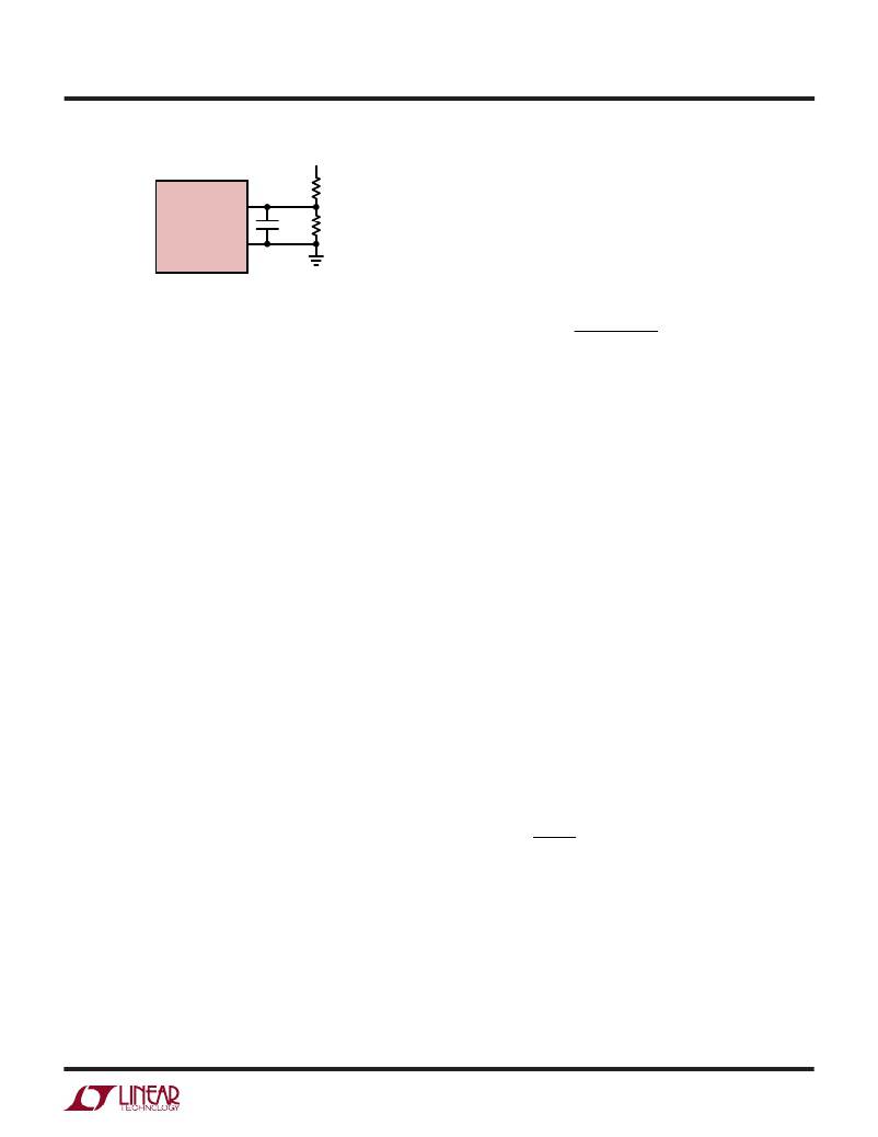
�LTC1735�
�APPLICATIO� S� I� FOR� ATIO�
�V� OUT�
�R2�
�V� OUT� resistive� divider.� The� maximum� current� flowing� out�
�of� the� sense� pins� is:�
�V� OSENSE�
�LTC1735�
�SGND�
�1735� F04�
�47pF�
�R1�
�I� SENSE+� +� I� SENSE–� =� (2.4V� –� V� OUT� )/24k�
�Since� V� OSENSE� is� servoed� to� the� 0.8V� reference� voltage,� we�
�can� choose� R1� in� Figure� 4� to� have� a� maximum� value� to�
�absorb� this� current:�
�R� 1� MAX� )� =� 24� k� ?� ?�
�Figure 4. Setting the LTC1735 Output Voltage�
�Topside� MOSFET� Driver� Supply� (C� B� ,� D� B� )�
�An� external� bootstrap� capacitor� C� B� connected� to� the�
�BOOST� pin� supplies� the� gate� drive� voltage� for� the� topside�
�MOSFET.� Capacitor� C� B� in� the� Functional� Diagram� is� charged�
�though� external� diode� D� B� from� INTV� CC� when� the� SW� pin�
�is� low.� Note� that� the� voltage� across� C� B� is� about� a� diode�
�drop� below� INTV� CC� .� When� the� topside� MOSFET� is� to� be�
�turned� on,� the� driver� places� the� C� B� voltage� across� the�
�gate-source� of� the� MOSFET.� This� enhances� the� MOSFET�
�and� turns� on� the� topside� switch.� The� switch� node� voltage�
�SW� rises� to� V� IN� and� the� BOOST� pin� rises� to� V� IN� +� INTV� CC� .�
�The� value� of� the� boost� capacitor� C� B� needs� to� be� 100� times�
�greater� than� the� total� input� capacitance� of� the� topside�
�MOSFET.� In� most� applications� 0.1� μ� F� to� 0.33� μ� F� is� ad-�
�equate.� The� reverse� breakdown� on� D� B� must� be� greater�
�than� V� IN(MAX)� .�
�When� adjusting� the� gate� drive� level,� the� final� arbiter� is� the�
�total� input� current� for� the� regulator.� If� you� make� a� change�
�and� the� input� current� decreases,� then� you� improved� the�
�efficiency.� If� there� is� no� change� in� input� current,� then� there�
�is� no� change� in� efficiency.�
�?� 0� .� 8� V� ?�
�?� 2� .� 4� V� –� V� OUT� ?�
�Regulating� an� output� voltage� of� 1.8V,� the� maximum� value�
�of� R1� should� be� 32k.� Note� that� at� output� voltages� above�
�2.4V� no� maximum� value� of� R1� is� necessary� to� absorb� the�
�sense� pin� currents;� however,� R1� is� still� bounded� by� the�
�V� OSENSE� feedback� current.�
�Soft-Start/Run� Function�
�The� RUN/SS� pin� is� a� multipurpose� pin� that� provides� a� soft-�
�start� function� and� a� means� to� shut� down� the� LTC1735.�
�Soft-start� reduces� surge� currents� from� V� IN� by� gradually�
�increasing� the� controller’s� current� limit� I� TH(MAX)� .� This� pin�
�can� also� be� used� for� power� supply� sequencing.�
�Pulling� the� RUN/SS� pin� below� 1.5V� puts� the� LTC1735� into�
�shutdown.� This� pin� can� be� driven� directly� from� logic� as�
�shown� in� Figure� 5.� The� V� IN� quiescent� current� is� a� function�
�of� RUN/SS� voltage� (refer� to� Typical� Performance� Charac-�
�teristics� graphs� on� page� 6).� Releasing� the� RUN/SS� pin�
�allows� an� internal� 1.2� μ� A� current� source� to� charge� up� the�
�external� soft-start� capacitor� C� SS.� If� RUN/SS� has� been�
�pulled� all� the� way� to� ground� there� is� a� delay� before� starting�
�t� DELAY� =�
�SENSE� +� /SENSE� –� Pins�
�The� common� mode� input� range� of� the� current� comparator�
�is� from� 0V� to� 1.1(INTV� CC� ).� Continuous� linear� operation� in�
�of� approximately:�
�1� .� 5� V�
�1� .� 2� μ� A�
�C� SS� =� (� 1� .� 25� s� /� μ� F� )� C� SS�
�step-down� applications� is� guaranteed� throughout� this�
�range� allowing� output� voltages� anywhere� from� 0.8V� to� 7V.�
�A� differential� NPN� input� stage� is� used� and� is� biased� with�
�internal� resistors� from� an� internal� 2.4V� source� as� shown�
�in� the� Functional� Diagram.� This� causes� current� to� either� be�
�sourced� or� sunk� by� the� sense� pins� depending� on� the�
�output� voltage.� If� the� output� voltage� is� below� 2.4V� current�
�will� flow� out� of� both� sense� pins� to� the� main� output.� This�
�forces� a� minimum� load� current� that� can� be� fulfilled� by� the�
�When� the� voltage� on� RUN/SS� reaches� 1.5V� the� LTC1735�
�begins� operating� with� a� current� limit� at� approximately�
�25mV/R� SENSE� .� As� the� voltage� on� the� RUN/SS� pin� increases�
�from� 1.5V� to� 3.0V,� the� internal� current� limit� is� increased�
�from� 25mV/R� SENSE� to� 75mV/R� SENSE� .� The� output� current�
�limit� ramps� up� slowly,� taking� an� additional� 1.25s/� μ� F� to�
�reach� full� current.� The� output� current� thus� ramps� up�
�slowly,� reducing� the� starting� surge� current� required� from�
�the� input� power� supply.�
�1735fc�
�17�
�相关PDF资料 |
PDF描述 |
|---|---|
| RSM15DREF | CONN EDGECARD 30POS .156 EYELET |
| MCP1703A-3002E/DB | IC REG LDO 3V .25A SOT-223-3 |
| 4922-10L | INDUCTOR 5.6UH POWER SMD |
| 4922-09L | INDUCTOR 4.7UH POWER SMD |
| MCP1703A-2802E/DB | IC REG LDO 2.8V .25A SOT-223-3 |
相关代理商/技术参数 |
参数描述 |
|---|---|
| LTC1736CG | 功能描述:IC SW REG STEP-DOWN SYNC 24-SSOP RoHS:否 类别:集成电路 (IC) >> PMIC - 稳压器 - 专用型 系列:- 标准包装:43 系列:- 应用:控制器,Intel VR11 输入电压:5 V ~ 12 V 输出数:1 输出电压:0.5 V ~ 1.6 V 工作温度:-40°C ~ 85°C 安装类型:表面贴装 封装/外壳:48-VFQFN 裸露焊盘 供应商设备封装:48-QFN(7x7) 包装:管件 |
| LTC1736CG#PBF | 功能描述:IC SW REG STEP-DONW SYNC 24-SSOP RoHS:是 类别:集成电路 (IC) >> PMIC - 稳压器 - 专用型 系列:- 标准包装:43 系列:- 应用:控制器,Intel VR11 输入电压:5 V ~ 12 V 输出数:1 输出电压:0.5 V ~ 1.6 V 工作温度:-40°C ~ 85°C 安装类型:表面贴装 封装/外壳:48-VFQFN 裸露焊盘 供应商设备封装:48-QFN(7x7) 包装:管件 |
| LTC1736CG#TR | 功能描述:IC REG SW SYNC STEPDWN HE 24SSOP RoHS:否 类别:集成电路 (IC) >> PMIC - 稳压器 - 专用型 系列:- 标准包装:43 系列:- 应用:控制器,Intel VR11 输入电压:5 V ~ 12 V 输出数:1 输出电压:0.5 V ~ 1.6 V 工作温度:-40°C ~ 85°C 安装类型:表面贴装 封装/外壳:48-VFQFN 裸露焊盘 供应商设备封装:48-QFN(7x7) 包装:管件 |
| LTC1736CG#TRPBF | 功能描述:IC SW REG STEP-DONW SYNC 24-SSOP RoHS:是 类别:集成电路 (IC) >> PMIC - 稳压器 - 专用型 系列:- 标准包装:43 系列:- 应用:控制器,Intel VR11 输入电压:5 V ~ 12 V 输出数:1 输出电压:0.5 V ~ 1.6 V 工作温度:-40°C ~ 85°C 安装类型:表面贴装 封装/外壳:48-VFQFN 裸露焊盘 供应商设备封装:48-QFN(7x7) 包装:管件 |
| LTC1736IG | 功能描述:IC REG SW SYNC STEPDWN HE 24SSOP RoHS:否 类别:集成电路 (IC) >> PMIC - 稳压器 - 专用型 系列:- 标准包装:43 系列:- 应用:控制器,Intel VR11 输入电压:5 V ~ 12 V 输出数:1 输出电压:0.5 V ~ 1.6 V 工作温度:-40°C ~ 85°C 安装类型:表面贴装 封装/外壳:48-VFQFN 裸露焊盘 供应商设备封装:48-QFN(7x7) 包装:管件 |
发布紧急采购,3分钟左右您将得到回复。