- 您现在的位置:买卖IC网 > PDF目录4952 > LTC1735IS#PBF (Linear Technology)IC REG CTRLR BUCK PWM CM 16-SOIC PDF资料下载
参数资料
| 型号: | LTC1735IS#PBF |
| 厂商: | Linear Technology |
| 文件页数: | 7/32页 |
| 文件大小: | 0K |
| 描述: | IC REG CTRLR BUCK PWM CM 16-SOIC |
| 标准包装: | 50 |
| PWM 型: | 电流模式 |
| 输出数: | 1 |
| 频率 - 最大: | 335kHz |
| 占空比: | 99.4% |
| 电源电压: | 4 V ~ 30 V |
| 降压: | 是 |
| 升压: | 无 |
| 回扫: | 无 |
| 反相: | 无 |
| 倍增器: | 无 |
| 除法器: | 无 |
| Cuk: | 无 |
| 隔离: | 无 |
| 工作温度: | -40°C ~ 85°C |
| 封装/外壳: | 16-SOIC(0.154",3.90mm 宽) |
| 包装: | 管件 |
| 产品目录页面: | 1333 (CN2011-ZH PDF) |
第1页第2页第3页第4页第5页第6页当前第7页第8页第9页第10页第11页第12页第13页第14页第15页第16页第17页第18页第19页第20页第21页第22页第23页第24页第25页第26页第27页第28页第29页第30页第31页第32页
�� �
�
�LTC1735�
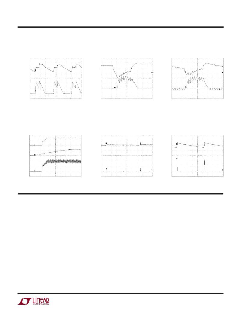
�TYPICAL� PERFOR� A� CE� CHARACTERISTICS�
�V� OUT(RIPPLE)�
�(Burst� Mode� Operation)�
�Load� Step� (Burst� Mode� Operation)�
�Load� Step� (Continuous� Mode)�
�V� OUT�
�20mV/DIV�
�I� LOAD� = 1.5A�
�FIGURE 1�
�V� OUT�
�FIGURE 1�
�V� OUT�
�50mV/DIV�
�FIGURE 1�
�50mV/DIV�
�I� L�
�I� L�
�I� L�
�5A/DIV�
�5A/DIV�
�5A/DIV�
�FCB� =� 5V�
�5� μ� s/DIV�
�1735� G27�
�10mA� TO�
�10� μ� s/DIV�
�1735� G26�
�0A� TO�
�10� μ� s/DIV�
�1735� G25�
�V� IN� =� 15V�
�V� OUT� =� 1.6V�
�Start-Up�
�9A� LOAD� STEP�
�FCB� =� 5V�
�V� IN� =� 15V�
�V� OUT� =� 1.6V�
�V� OUT(RIPPLE)� (Synchronized)�
�9A� LOAD� STEP�
�FCB� =� 0V�
�V� IN� =� 15V�
�V� OUT� =� 1.6V�
�V� OUT(RIPPLE)�
�(Burst� Mode� Operation)�
�V� OUT�
�1V/DIV�
�V� OUT�
�10mV/DIV�
�I� LOAD� = 10mA�
�FIGURE 1�
�V� OUT�
�20mV/DIV�
�I� LOAD� = 50mA�
�FIGURE 1�
�V� RUN/SS�
�5V/DIV�
�I� L�
�I� L�
�5A/DIV�
�I� L�
�5A/DIV�
�5A/DIV�
�V� IN� =� 15V�
�5ms/DIV�
�1735� G22�
�EXT� SYNC� f� =� f� O�
�10� μ� s/DIV�
�1735� G23�
�FCB� =� 5V�
�50� μ� s/DIV�
�1735� G24�
�V� OUT� =� 1.6V�
�R� LOAD� =� 0.16� ?�
�PI� FU� CTIO� S�
�V� IN� =� 15V�
�V� OUT� =� 1.6V�
�V� IN� =� 15V�
�V� OUT� =� 1.6V�
�C� OSC� :� External� capacitor� C� OSC� from� this� pin� to� ground� sets�
�the� operating� frequency.�
�RUN/SS:� Combination� of� Soft-Start� and� Run� Control� In-�
�puts.� A� capacitor� to� ground� at� this� pin� sets� the� ramp� time�
�to� full� output� current.� The� time� is� approximately� 1.25s/� μ� F.�
�Forcing� this� pin� below� 1.5V� causes� the� device� to� shut�
�down.� (See� Applications� Information� section� for� quiescent�
�current� note.)� In� shutdown� all� functions,� including� INTV� CC� ,�
�are� disabled.� Latchoff� overcurrent� protection� is� also� in-�
�voked� via� this� pin� as� described� in� the� Applications� Infor-�
�mation� section.�
�I� TH� :� Error� Amplifier� Compensation� Point.� The� current�
�comparator� threshold� increases� with� this� control� voltage.�
�Nominal� voltage� range� for� this� pin� is� 0V� to� 2.4V.�
�FCB:� Forced� Continuous/Synchronization� Input.� Tie� this�
�pin� to� ground� for� continuous� synchronous� operation,� to� a�
�resistive� divider� from� the� secondary� output� when� using� a�
�secondary� winding� or� to� INTV� CC� to� enable� Burst� Mode�
�operation� at� low� load� currents.� Clocking� this� pin� with� a�
�signal� above� 1.5V� P–P� disables� Burst� Mode� operation� but�
�allows� cycle-skipping� at� low� load� currents� and� synchro-�
�nizes� the� internal� oscillator� with� the� external� clock.� The�
�FCB� pin� must� not� be� driven� when� the� device� is� shut� down�
�(RUN/SS� pin� low).�
�SGND:� Small-Signal� Ground.� All� small-signal� components�
�such� as� C� OSC� ,� C� SS� ,� the� feedback� divider� plus� the� loop� com-�
�pensation� resistor� and� capacitor(s)� should� single-point� tie�
�to� this� pin.� This� pin� should,� in� turn,� connect� to� PGND.�
�1735fc�
�7�
�相关PDF资料 |
PDF描述 |
|---|---|
| RSM15DREF | CONN EDGECARD 30POS .156 EYELET |
| MCP1703A-3002E/DB | IC REG LDO 3V .25A SOT-223-3 |
| 4922-10L | INDUCTOR 5.6UH POWER SMD |
| 4922-09L | INDUCTOR 4.7UH POWER SMD |
| MCP1703A-2802E/DB | IC REG LDO 2.8V .25A SOT-223-3 |
相关代理商/技术参数 |
参数描述 |
|---|---|
| LTC1736CG | 功能描述:IC SW REG STEP-DOWN SYNC 24-SSOP RoHS:否 类别:集成电路 (IC) >> PMIC - 稳压器 - 专用型 系列:- 标准包装:43 系列:- 应用:控制器,Intel VR11 输入电压:5 V ~ 12 V 输出数:1 输出电压:0.5 V ~ 1.6 V 工作温度:-40°C ~ 85°C 安装类型:表面贴装 封装/外壳:48-VFQFN 裸露焊盘 供应商设备封装:48-QFN(7x7) 包装:管件 |
| LTC1736CG#PBF | 功能描述:IC SW REG STEP-DONW SYNC 24-SSOP RoHS:是 类别:集成电路 (IC) >> PMIC - 稳压器 - 专用型 系列:- 标准包装:43 系列:- 应用:控制器,Intel VR11 输入电压:5 V ~ 12 V 输出数:1 输出电压:0.5 V ~ 1.6 V 工作温度:-40°C ~ 85°C 安装类型:表面贴装 封装/外壳:48-VFQFN 裸露焊盘 供应商设备封装:48-QFN(7x7) 包装:管件 |
| LTC1736CG#TR | 功能描述:IC REG SW SYNC STEPDWN HE 24SSOP RoHS:否 类别:集成电路 (IC) >> PMIC - 稳压器 - 专用型 系列:- 标准包装:43 系列:- 应用:控制器,Intel VR11 输入电压:5 V ~ 12 V 输出数:1 输出电压:0.5 V ~ 1.6 V 工作温度:-40°C ~ 85°C 安装类型:表面贴装 封装/外壳:48-VFQFN 裸露焊盘 供应商设备封装:48-QFN(7x7) 包装:管件 |
| LTC1736CG#TRPBF | 功能描述:IC SW REG STEP-DONW SYNC 24-SSOP RoHS:是 类别:集成电路 (IC) >> PMIC - 稳压器 - 专用型 系列:- 标准包装:43 系列:- 应用:控制器,Intel VR11 输入电压:5 V ~ 12 V 输出数:1 输出电压:0.5 V ~ 1.6 V 工作温度:-40°C ~ 85°C 安装类型:表面贴装 封装/外壳:48-VFQFN 裸露焊盘 供应商设备封装:48-QFN(7x7) 包装:管件 |
| LTC1736IG | 功能描述:IC REG SW SYNC STEPDWN HE 24SSOP RoHS:否 类别:集成电路 (IC) >> PMIC - 稳压器 - 专用型 系列:- 标准包装:43 系列:- 应用:控制器,Intel VR11 输入电压:5 V ~ 12 V 输出数:1 输出电压:0.5 V ~ 1.6 V 工作温度:-40°C ~ 85°C 安装类型:表面贴装 封装/外壳:48-VFQFN 裸露焊盘 供应商设备封装:48-QFN(7x7) 包装:管件 |
发布紧急采购,3分钟左右您将得到回复。