- 您现在的位置:买卖IC网 > PDF目录15248 > LTC1876EG (Linear Technology)IC REG CTRLR BST PWM CM 36-SSOP PDF资料下载
参数资料
| 型号: | LTC1876EG |
| 厂商: | Linear Technology |
| 文件页数: | 20/36页 |
| 文件大小: | 0K |
| 描述: | IC REG CTRLR BST PWM CM 36-SSOP |
| 标准包装: | 37 |
| 系列: | PolyPhase® |
| PWM 型: | 电流模式 |
| 输出数: | 3 |
| 频率 - 最大: | 360kHz |
| 占空比: | 99.4% |
| 电源电压: | 3.5 V ~ 36 V |
| 降压: | 是 |
| 升压: | 是 |
| 回扫: | 无 |
| 反相: | 无 |
| 倍增器: | 无 |
| 除法器: | 无 |
| Cuk: | 无 |
| 隔离: | 无 |
| 工作温度: | -40°C ~ 85°C |
| 封装/外壳: | 36-SSOP(0.209",5.30mm 宽) |
| 包装: | 管件 |
第1页第2页第3页第4页第5页第6页第7页第8页第9页第10页第11页第12页第13页第14页第15页第16页第17页第18页第19页当前第20页第21页第22页第23页第24页第25页第26页第27页第28页第29页第30页第31页第32页第33页第34页第35页第36页
�� �
�
�LTC1876�
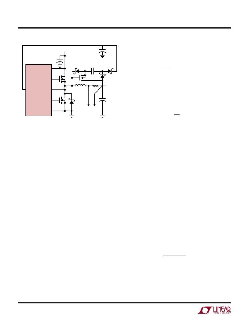
�APPLICATIO� S� I� FOR� ATIO�
�+�
�V� IN�
�+�
�1� μ� F�
�the� internal� precision� 0.8V� voltage� reference� by� the� error�
�amplifier.� The� output� voltage� is� given� by� the� equation:�
�V� OUT� =� 0� .� 8� V� ?� 1� +� ?�
�LTC1876�
�EXTV� CC�
�V� IN�
�TG1�
�SW�
�BG1�
�C� IN�
�N-CH�
�BAT85�
�L1�
�0.22� μ� F�
�VN2222LL�
�R� SENSE�
�+�
�BAT85�
�BAT85�
�V� OUT�
�C� OUT�
�?� R� 2� ?�
�?� R� 1� ?�
�For� the� auxillary� boost� regulator,� the� resultant� feedback�
�signal� is� compared� with� the� internal� precision� 1.26V�
�voltage� reference� by� the� error� amplifier.� The� output� volt-�
�age� is� given� by� the� equation:�
�V� OUTAUX� =� 1� .� 26� V� ?� 1� +�
�R� 7� ?�
�PGND�
�N-CH�
�1876� F06b�
�?�
�?�
�R� 8� ?�
�?�
�R� 1� MAX� )� =� 24� k� ?� ?�
�Figure 6b. Capacitive Charge Pump for EXTV� CC�
�Topside� MOSFET� Driver� Supply� (C� B� ,� D� B� )�
�External� bootstrap� capacitors� C� B� connected� to� the� BOOST�
�pins� supply� the� gate� drive� voltages� for� the� topside� MOS-�
�FETs.� Capacitor� C� B� in� the� functional� diagram� is� charged�
�though� external� diode� D� B� from� INTV� CC� when� the� SW� pin� is�
�low.� When� one� of� the� topside� MOSFETs� is� to� be� turned� on,�
�the� driver� places� the� C� B� voltage� across� the� gate-source� of�
�the� desired� MOSFET.� This� enhances� the� MOSFET� and�
�turns� on� the� topside� switch.� The� switch� node� voltage,� SW,�
�rises� to� V� IN� and� the� BOOST� pin� follows.� With� the� topside�
�MOSFET� on,� the� boost� voltage� is� above� the� input� supply:�
�V� BOOST� =� V� IN� +� V� INTVCC� .� The� value� of� the� boost� capacitor�
�C� B� needs� to� be� 100� times� that� of� the� total� input� capacitance�
�of� the� topside� MOSFET(s).� The� reverse� breakdown� of� the�
�external� Schottky� diode� must� be� greater� than� V� IN(MAX)� .�
�When� adjusting� the� gate� drive� level,� the� final� arbiter� is� the�
�total� input� current� for� the� regulator.� If� a� change� is� made�
�and� the� input� current� decreases,� then� the� efficiency� has�
�improved.� If� there� is� no� change� in� input� current,� then� there�
�is� no� change� in� efficiency.�
�Output� Voltage�
�The� LTC1876� output� voltages� are� each� set� by� an� external�
�feedback� resistive� divider� carefully� placed� across� the�
�output� capacitor� as� shown� in� Figure� 2.� For� the� step-down�
�controller,� the� resultant� feedback� signal� is� compared� with�
�SENSE� +� /SENSE� –� Pins�
�The� common� mode� input� range� of� the� current� comparator�
�SENSE� pins� is� from� 0V� to� (1.1)INTV� CC� .� Continuous� linear�
�operation� is� guaranteed� throughout� this� range� allowing�
�output� voltage� setting� from� 0.8V� to� 7.7V,� depending� upon�
�the� voltage� applied� to� EXTV� CC� .� A� differential� NPN� input�
�stage� is� biased� with� internal� resistors� from� an� internal� 2.4V�
�source� as� shown� in� the� Functional� Diagram.� This� requires�
�that� current� either� be� sourced� or� sunk� from� the� SENSE�
�pins� depending� on� the� output� voltage.� If� the� output� voltage�
�is� below� 2.4V� current� will� flow� out� of� both� SENSE� pins� to�
�the� main� output.� The� output� can� be� easily� preloaded� by� the�
�V� OUT� resistive� divider� to� compensate� for� the� current�
�comparator’s� negative� input� bias� current.� The� maximum�
�current� flowing� out� of� each� pair� of� SENSE� pins� is:�
�I� SENSE+� +� I� SENSE–� =� (2.4V� –� V� OUT� )/24k�
�Since� V� OSENSE� is� servoed� to� the� 0.8V� reference� voltage,� we�
�can� choose� R1� in� Figure� 2� to� have� a� maximum� value� to�
�absorb� this� current.�
�?� 0� .� 8� V� ?�
�?� 2� .� 4� V� –� V� OUT� ?�
�for� V� OUT� <� 2.4V�
�Regulating� an� output� voltage� of� 1.8V,� the� minimum� value�
�of� R1� should� be� 32k.� Note� that� for� an� output� voltage� above�
�2.4V,� R1� has� no� maximum� value� since� the� SENSE� pins�
�load� the� output.�
�1876fa�
�20�
�相关PDF资料 |
PDF描述 |
|---|---|
| LTC1876EG#PBF | IC REG CTRLR BST PWM CM 36-SSOP |
| CAT809MTBI-T3 | IC VOLTAGE SUPERVISOR SOT-23-3 |
| ELL-3GM3R9N | COIL PWR CHOKE 3.9UH 940MA SMD |
| CAT809JTBI-T3 | IC VOLTAGE SUPERVISOR SOT-23-3 |
| ELL-3GM3R3N | COIL PWR CHOKE 3.3UH 980MA SMD |
相关代理商/技术参数 |
参数描述 |
|---|---|
| LTC1876EG#PBF | 功能描述:IC REG CTRLR BST PWM CM 36-SSOP RoHS:是 类别:集成电路 (IC) >> PMIC - 稳压器 - DC DC 切换控制器 系列:PolyPhase® 标准包装:4,500 系列:PowerWise® PWM 型:控制器 输出数:1 频率 - 最大:1MHz 占空比:95% 电源电压:2.8 V ~ 5.5 V 降压:是 升压:无 回扫:无 反相:无 倍增器:无 除法器:无 Cuk:无 隔离:无 工作温度:-40°C ~ 125°C 封装/外壳:6-WDFN 裸露焊盘 包装:带卷 (TR) 配用:LM1771EVAL-ND - BOARD EVALUATION LM1771 其它名称:LM1771SSDX |
| LTC1876EG#TR | 功能描述:IC REG CTRLR BST PWM CM 36-SSOP RoHS:否 类别:集成电路 (IC) >> PMIC - 稳压器 - DC DC 切换控制器 系列:PolyPhase® 标准包装:4,500 系列:PowerWise® PWM 型:控制器 输出数:1 频率 - 最大:1MHz 占空比:95% 电源电压:2.8 V ~ 5.5 V 降压:是 升压:无 回扫:无 反相:无 倍增器:无 除法器:无 Cuk:无 隔离:无 工作温度:-40°C ~ 125°C 封装/外壳:6-WDFN 裸露焊盘 包装:带卷 (TR) 配用:LM1771EVAL-ND - BOARD EVALUATION LM1771 其它名称:LM1771SSDX |
| LTC1876EG#TRPBF | 功能描述:IC REG CTRLR BST PWM CM 36-SSOP RoHS:是 类别:集成电路 (IC) >> PMIC - 稳压器 - DC DC 切换控制器 系列:PolyPhase® 标准包装:4,500 系列:PowerWise® PWM 型:控制器 输出数:1 频率 - 最大:1MHz 占空比:95% 电源电压:2.8 V ~ 5.5 V 降压:是 升压:无 回扫:无 反相:无 倍增器:无 除法器:无 Cuk:无 隔离:无 工作温度:-40°C ~ 125°C 封装/外壳:6-WDFN 裸露焊盘 包装:带卷 (TR) 配用:LM1771EVAL-ND - BOARD EVALUATION LM1771 其它名称:LM1771SSDX |
| LTC1877EMS8 | 功能描述:IC REG BUCK SYNC ADJ 0.6A 8MSOP RoHS:否 类别:集成电路 (IC) >> PMIC - 稳压器 - DC DC 开关稳压器 系列:- 标准包装:2,500 系列:- 类型:降压(降压) 输出类型:固定 输出数:1 输出电压:1.2V,1.5V,1.8V,2.5V 输入电压:2.7 V ~ 20 V PWM 型:- 频率 - 开关:- 电流 - 输出:50mA 同步整流器:是 工作温度:-40°C ~ 125°C 安装类型:表面贴装 封装/外壳:10-TFSOP,10-MSOP(0.118",3.00mm 宽)裸露焊盘 包装:带卷 (TR) 供应商设备封装:10-MSOP 裸露焊盘 |
| LTC1877EMS8#PBF | 功能描述:IC REG BUCK SYNC ADJ 0.6A 8MSOP RoHS:是 类别:集成电路 (IC) >> PMIC - 稳压器 - DC DC 开关稳压器 系列:- 标准包装:250 系列:- 类型:降压(降压) 输出类型:固定 输出数:1 输出电压:1.2V 输入电压:2.05 V ~ 6 V PWM 型:电压模式 频率 - 开关:2MHz 电流 - 输出:500mA 同步整流器:是 工作温度:-40°C ~ 85°C 安装类型:表面贴装 封装/外壳:6-UFDFN 包装:带卷 (TR) 供应商设备封装:6-SON(1.45x1) 产品目录页面:1032 (CN2011-ZH PDF) 其它名称:296-25628-2 |
发布紧急采购,3分钟左右您将得到回复。