- 您现在的位置:买卖IC网 > PDF目录39414 > LTC2206UK-14#TR (LINEAR TECHNOLOGY CORP) PROPRIETARY METHOD ADC, PQCC48 PDF资料下载
参数资料
| 型号: | LTC2206UK-14#TR |
| 厂商: | LINEAR TECHNOLOGY CORP |
| 元件分类: | ADC |
| 英文描述: | PROPRIETARY METHOD ADC, PQCC48 |
| 封装: | 7 X 7 MM, PLASTIC, MO-220WKKD-2, QFN-48 |
| 文件页数: | 15/32页 |
| 文件大小: | 1307K |
| 代理商: | LTC2206UK-14#TR |
第1页第2页第3页第4页第5页第6页第7页第8页第9页第10页第11页第12页第13页第14页当前第15页第16页第17页第18页第19页第20页第21页第22页第23页第24页第25页第26页第27页第28页第29页第30页第31页第32页
LTC2207-14/LTC2206-14
22
220714614fa
An optional clock duty cycle stabilizer can be used if the
input clock does not have a 50% duty cycle. This circuit
uses the rising edge of ENC pin to sample the analog input.
The falling edge of ENC is ignored and an internal falling
edge is generated by a phase-locked loop. The input clock
duty cycle can vary from 30% to 70% and the clock duty
cycle stabilizer will maintain a constant 50% internal duty
cycle. If the clock is turned off for a long period of time,
the duty cycle stabilizer circuit will require one hundred
clock cycles for the PLL to lock onto the input clock. To
use the clock duty cycle stabilizer, the MODE pin must be
connected to 1/3VDD or 2/3VDD using external resistors.
The lower limit of the LTC2207-14/LTC2206-14 sample rate
is determined by droop of the sample and hold circuits. The
pipelined architecture of this ADC relies on storing analog
signals on small valued capacitors. Junction leakage will
discharge the capacitors. The specied minimum operating
frequency for the LTC2207-14/LTC2206-14 is 1Msps.
DIGITAL OUTPUTS
Digital Output Buffers
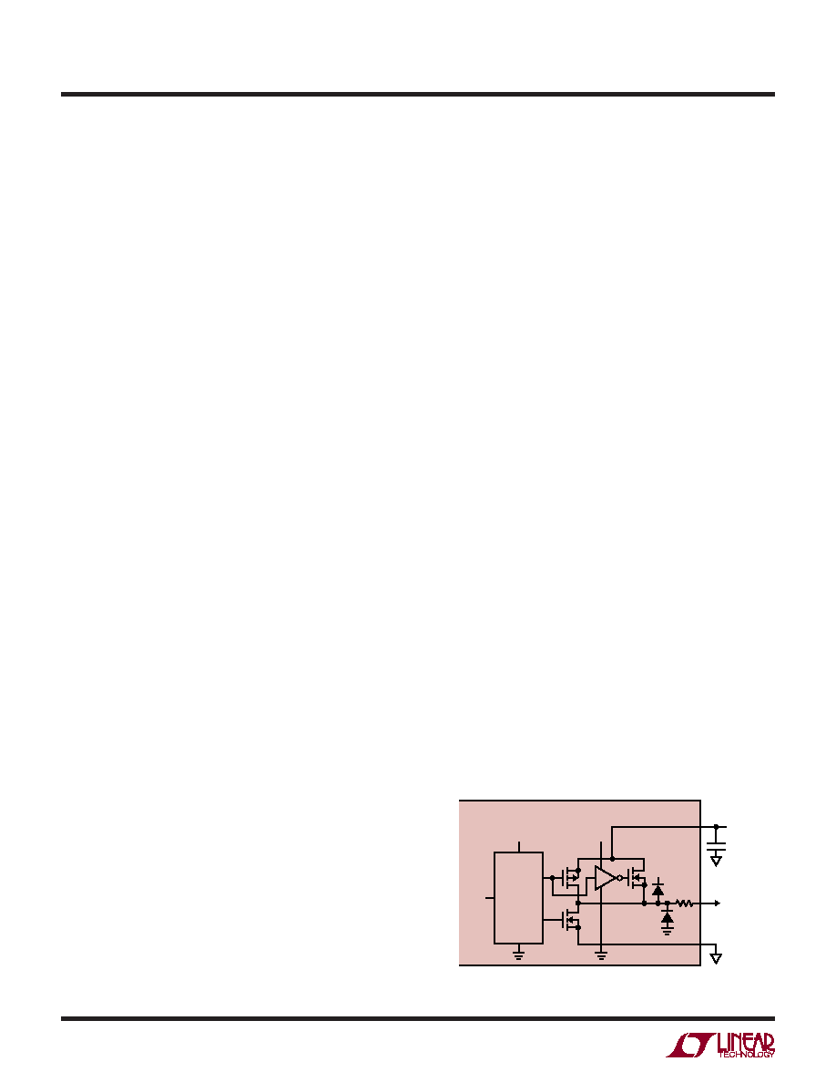
Figure 11 shows an equivalent circuit for a single output
buffer. Each buffer is powered by OVDD and OGND, isolated
from the ADC power and ground. The additional N-channel
transistor in the output driver allows operation down to
low voltages. The internal resistor in series with the output
eliminates the need for external damping resistors.
As with all high speed/high resolution converters, the
digital output loading can affect the performance. The
digital outputs of the LTC2207-14/LTC2206-14 should drive
a minimum capacitive load to avoid possible interaction
between the digital outputs and sensitive input circuitry.
Driving the Encode Inputs
The noise performance of the LTC2207-14/LTC2206-14
can depend on the encode signal quality as much as on the
analog input. The encode inputs are intended to be driven
differentially, primarily for noise immunity from common
mode noise sources. Each input is biased through a 6k
resistor to a 1.6V bias. The bias resistors set the DC oper-
ating point for transformer coupled drive circuits and can
set the logic threshold for single-ended drive circuits.
Any noise present on the encode signal will result in ad-
ditional aperture jitter that will be RMS summed with the
inherent ADC aperture jitter.
In applications where jitter is critical (high input frequen-
cies), take the following into consideration:
1. Differential drive should be used.
2. Use as large an amplitude possible. If using trans-
former coupling, use a higher turns ratio to increase the
amplitude.
3. If the ADC is clocked with a xed frequency sinusoidal
signal, lter the encode signal to reduce wideband
noise.
4. Balance the capacitance and series resistance at both
encode inputs such that any coupled noise will appear
at both inputs as common mode noise.
The encode inputs have a common mode range of 1.4V
to 3V. Each input may be driven from ground to VDD for
single-ended drive.
Maximum and Minimum Encode Rates
The maximum encode rate for the LTC2207-14 is 105Msps.
The maximum encode rate for the LTC2206-14 is 80Msps.
For the ADC to operate properly the encode signal should
have a 50% (±5%) duty cycle. Each half cycle must be at
least 4.52ns for the LTC2207-14 internal circuitry to have
enough settling time for proper operation. For the LTC2206-
14, each half cycle must be at least 5.94ns. Achieving a
precise 50% duty cycle is easy with differential sinusoidal
drive using a transformer or using symmetric differential
logic such as PECL or LVDS. When using a single-ended
ENCODE signal asymmetric rise and fall times can result
in duty cycles that are far from 50%.
APPLICATIONS INFORMATION
LTC2207-14/LTC2206-14
22076 F11
OVDD
VDD
0.1
F
TYPICAL
DATA
OUTPUT
OGND
OVDD
0.5V
TO 3.6V
PREDRIVER
LOGIC
DATA
FROM
LATCH
33
Figure 11. Equivalent Circuit for a Digital Output Buffer
相关PDF资料 |
PDF描述 |
|---|---|
| LTC2207UK-14#TRPBF | PROPRIETARY METHOD ADC, PQCC48 |
| LTC2207UK-14#TR | PROPRIETARY METHOD ADC, PQCC48 |
| LTC2207UK-14#PBF | PROPRIETARY METHOD ADC, PQCC48 |
| LTC2209IUP | 1-CH 16-BIT PROPRIETARY METHOD ADC, PARALLEL ACCESS, PQCC64 |
| LTC2215CUP | 1-CH 16-BIT PROPRIETARY METHOD ADC, PARALLEL ACCESS, PQCC64 |
相关代理商/技术参数 |
参数描述 |
|---|---|
| LTC2207 | 制造商:LINER 制造商全称:Linear Technology 功能描述:16-Bit, 20Msps Low Power ADC |
| LTC2207-14 | 制造商:LINER 制造商全称:Linear Technology 功能描述:14-Bit, 105Msps/80Msps ADCs |
| LTC2207CUK | 制造商:Linear Technology 功能描述:ADC Single Pipelined 105Msps 16-bit Parallel 48-Pin QFN EP |
| LTC2207CUK#PBF | 制造商:Linear Technology 功能描述:ADC Single Pipelined 105Msps 16-bit Parallel 48-Pin QFN EP 制造商:Linear Technology 功能描述:IC ADC 16-BIT 105MSPS 48-QFN 制造商:Linear Technology 功能描述:IC ADC 16BIT 105MSPS QFN-48 制造商:Linear Technology 功能描述:ADC 16BIT 105MSPS 48QFN 制造商:Linear Technology 功能描述:IC, ADC, 16BIT, 105MSPS, QFN-48; Resolution (Bits):16bit; Sampling Rate:105MSPS; Supply Voltage Type:Single; Supply Voltage Min:3.135V; Supply Voltage Max:3.465V; Supply Current:273mA; Digital IC Case Style:QFN; No. of Pins:48 ;RoHS Compliant: Yes |
| LTC2207CUK#PBF | 制造商:Linear Technology 功能描述:IC, ADC, 16BIT, 105MSPS, QFN-48 |
发布紧急采购,3分钟左右您将得到回复。