- 您现在的位置:买卖IC网 > PDF目录39414 > LTC2206UK-14#TR (LINEAR TECHNOLOGY CORP) PROPRIETARY METHOD ADC, PQCC48 PDF资料下载
参数资料
| 型号: | LTC2206UK-14#TR |
| 厂商: | LINEAR TECHNOLOGY CORP |
| 元件分类: | ADC |
| 英文描述: | PROPRIETARY METHOD ADC, PQCC48 |
| 封装: | 7 X 7 MM, PLASTIC, MO-220WKKD-2, QFN-48 |
| 文件页数: | 16/32页 |
| 文件大小: | 1307K |
| 代理商: | LTC2206UK-14#TR |
第1页第2页第3页第4页第5页第6页第7页第8页第9页第10页第11页第12页第13页第14页第15页当前第16页第17页第18页第19页第20页第21页第22页第23页第24页第25页第26页第27页第28页第29页第30页第31页第32页
LTC2207-14/LTC2206-14
23
220714614fa
The output should be buffered with a device such as a
ALVCH16373 CMOS latch. For full speed operation the
capacitive load should be kept under 10pF. A resistor in
series with the output may be used but is not required since
the output buffer has a series resistor of 33
Ω on chip.
Lower OVDD voltages will also help reduce interference
from the digital outputs.
Data Format
The LTC2207-14/LTC2206-14 parallel digital output can
be selected for offset binary or 2’s complement format.
The format is selected with the MODE pin. This pin has a
four level logic input, centered at 0, 1/3VDD, 2/3VDD and
VDD. An external resistor divider can be used to set the
1/3VDD and 2/3VDD logic levels. Table 1 shows the logic
states for the MODE pin.
Table 1. MODE Pin Function
MODE
Output Format
Clock Duty Cycle Stabilizer
0(GND)
Offset Binary
Off
1/3VDD
Offset Binary
On
2/3VDD
2’s Complement
On
VDD
2’s Complement
Off
Overow Bit
An overow output bit (OF) indicates when the converter
is over-ranged or under-ranged. A logic high on the OF
pin indicates an overow or underow.
Output Clock
The ADC has a delayed version of the encode input available
as a digital output. Both a noninverted version, CLKOUT+
and an inverted version CLKOUT– are provided. The
CLKOUT+/CLKOUT– can be used to synchronize the con-
verter data to the digital system. This is necessary when
using a sinusoidal encode. Data can be latched on the
rising edge of CLKOUT+ or the falling edge of CLKOUT–.
CLKOUT+ falls and CLKOUT– rises as the data outputs
are updated.
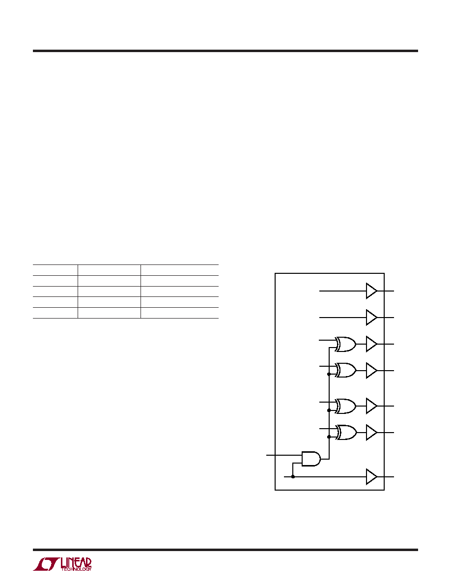
Digital Output Randomizer
Interference from the ADC digital outputs is sometimes
unavoidable. Interference from the digital outputs may be
from capacitive or inductive coupling or coupling through
the ground plane. Even a tiny coupling factor can result in
discernible unwanted tones in the ADC output spectrum.
By randomizing the digital output before it is transmitted
off chip, these unwanted tones can be randomized, trading
a slight increase in the noise oor for a large reduction in
unwanted tone amplitude.
The digital output is “Randomized” by applying an exclu-
sive-OR logic operation between the LSB and all other data
output bits. To decode, the reverse operation is applied;
that is, an exclusive-OR operation is applied between the
LSB and all other bits. The LSB, OF and CLKOUT outputs
are not affected. The output Randomizer function is active
when the RAND pin is high.
Figure 12. Functional Equivalent of Digital Output Randomizer
CLKOUT+
OF
D13/D0
D12/D0
D2/D0
D1/D0
D0
D1
RAND = HIGH,
SCRAMBLE
ENABLED
D2
D12
D13
OF
LTC2207-14/LTC2206-14
CLKOUT
RAND
22076 F12
APPLICATIONS INFORMATION
相关PDF资料 |
PDF描述 |
|---|---|
| LTC2207UK-14#TRPBF | PROPRIETARY METHOD ADC, PQCC48 |
| LTC2207UK-14#TR | PROPRIETARY METHOD ADC, PQCC48 |
| LTC2207UK-14#PBF | PROPRIETARY METHOD ADC, PQCC48 |
| LTC2209IUP | 1-CH 16-BIT PROPRIETARY METHOD ADC, PARALLEL ACCESS, PQCC64 |
| LTC2215CUP | 1-CH 16-BIT PROPRIETARY METHOD ADC, PARALLEL ACCESS, PQCC64 |
相关代理商/技术参数 |
参数描述 |
|---|---|
| LTC2207 | 制造商:LINER 制造商全称:Linear Technology 功能描述:16-Bit, 20Msps Low Power ADC |
| LTC2207-14 | 制造商:LINER 制造商全称:Linear Technology 功能描述:14-Bit, 105Msps/80Msps ADCs |
| LTC2207CUK | 制造商:Linear Technology 功能描述:ADC Single Pipelined 105Msps 16-bit Parallel 48-Pin QFN EP |
| LTC2207CUK#PBF | 制造商:Linear Technology 功能描述:ADC Single Pipelined 105Msps 16-bit Parallel 48-Pin QFN EP 制造商:Linear Technology 功能描述:IC ADC 16-BIT 105MSPS 48-QFN 制造商:Linear Technology 功能描述:IC ADC 16BIT 105MSPS QFN-48 制造商:Linear Technology 功能描述:ADC 16BIT 105MSPS 48QFN 制造商:Linear Technology 功能描述:IC, ADC, 16BIT, 105MSPS, QFN-48; Resolution (Bits):16bit; Sampling Rate:105MSPS; Supply Voltage Type:Single; Supply Voltage Min:3.135V; Supply Voltage Max:3.465V; Supply Current:273mA; Digital IC Case Style:QFN; No. of Pins:48 ;RoHS Compliant: Yes |
| LTC2207CUK#PBF | 制造商:Linear Technology 功能描述:IC, ADC, 16BIT, 105MSPS, QFN-48 |
发布紧急采购,3分钟左右您将得到回复。