- 您现在的位置:买卖IC网 > PDF目录296330 > LTC2208CUP#PBF (LINEAR TECHNOLOGY CORP) 16-Bit, 130Msps ADC; Package: QFN; No of Pins: 64; Temperature Range: 0°C to +70°C PDF资料下载
参数资料
| 型号: | LTC2208CUP#PBF |
| 厂商: | LINEAR TECHNOLOGY CORP |
| 元件分类: | ADC |
| 英文描述: | 16-Bit, 130Msps ADC; Package: QFN; No of Pins: 64; Temperature Range: 0°C to +70°C |
| 中文描述: | 1-CH 16-BIT PROPRIETARY METHOD ADC, PARALLEL ACCESS, PQCC64 |
| 封装: | 9 X 9 MM, LEAD FREE, PLASTIC, MO-220WNJR-5, QFN-64 |
| 文件页数: | 11/32页 |
| 文件大小: | 959K |
| 代理商: | LTC2208CUP#PBF |
第1页第2页第3页第4页第5页第6页第7页第8页第9页第10页当前第11页第12页第13页第14页第15页第16页第17页第18页第19页第20页第21页第22页第23页第24页第25页第26页第27页第28页第29页第30页第31页第32页
LTC2208
19
2208fc
input change is large, such as the change seen with input
frequencies near Nyquist, then a larger charging glitch
will be seen.
Common Mode Bias
The ADC sample-and-hold circuit requires differential
drive to achieve specied performance. Each input should
swing ±0.5625V for the 2.25V range (PGA = 0) or ±0.375V
for the 1.5V range (PGA = 1), around a common mode
voltage of 1.25V. The VCM output pin (Pin 3) is designed
to provide the common mode bias level. VCM can be tied
directly to the center tap of a transformer to set the DC
input level or as a reference level to an op amp differential
driver circuit. The VCM pin must be bypassed to ground
close to the ADC with 2.2μF or greater.
Input Drive Impedence
As with all high performance, high speed ADCs the dy-
namic performance of the LTC2208 can be inuenced
by the input drive circuitry, particularly the second and
third harmonics. Source impedance and input reactance
can inuence SFDR. At the falling edge of ENC the
sample and hold circuit will connect the 4.9pF sampling
capacitor to the input pin and start the sampling period.
The sampling period ends when ENC rises, holding the
sampled input on the sampling capacitor. Ideally, the
input circuitry should be fast enough to fully charge
the sampling capacitor during the sampling period
1/(2F encode); however, this is not always possible and the
incomplete settling may degrade the SFDR. The sampling
glitch has been designed to be as linear as possible to
minimize the effects of incomplete settling.
For the best performance it is recommended to have a
source impedence of 100
Ω or less for each input. The
source impedence should be matched for the differential
inputs. Poor matching will result in higher even order
harmonics, especially the second.
INPUT DRIVE CIRCUITS
Input Filtering
A rst order RC low pass lter at the input of the ADC can
serve two functions: limit the noise from input circuitry and
provide isolation from ADC S/H switching. The LTC2208
has a very broadband S/H circuit, DC to 700MHz; it can
be used in a wide range of applications; therefore, it is not
possible to provide a single recommended RC lter.
Figures 3, 4a and 4b show three examples of input RC
ltering at three ranges of input frequencies. In general
it is desirable to make the capacitors as large as can be
tolerated—this will help suppress random noise as well
as noise coupled from the digital circuitry. The LTC2208
does not require any input lter to achieve data sheet
specications; however, no ltering will put more stringent
noise requirements on the input drive circuitry.
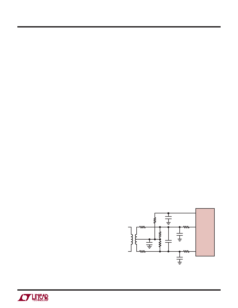
Transformer Coupled Circuits
Figure 3 shows the LTC2208 being driven by an RF trans-
former with a center-tapped secondary. The secondary
center tap is DC biased with VCM, setting the ADC input
signal at its optimum DC level. Figure 3 shows a 1:1 turns
ratio transformer. Other turns ratios can be used; however,
as the turns ratio increases so does the impedance seen by
the ADC. Source impedance greater than 50
Ω can reduce
the input bandwidth and increase high frequency distor-
tion. A disadvantage of using a transformer is the loss of
low frequency response. Most small RF transformers have
poor performance at frequencies below 1MHz.
Center-tapped transformers provide a convenient means
of DC biasing the secondary; however, they often show
poor balance at high input frequencies, resulting in large
2nd order harmonics.
Figure 3. Single-Ended to Differential Conversion
Using a Transformer. Recommended for Input
Frequencies from 5MHz to 100MHz
35Ω
5Ω
35Ω
10Ω
5Ω
0.1μF
AIN
+
AIN
–
8.2pF
2.2μF
8.2pF
VCM
LTC2208
T1
T1 = MA/COM ETC1-1T
RESISTORS, CAPACITORS
ARE 0402 PACKAGE SIZE
EXCEPT 2.2μF
2208 F03
APPLICATIONS INFORMATION
相关PDF资料 |
PDF描述 |
|---|---|
| LTC2208CUP#TRPBF | 16-Bit, 130Msps ADC; Package: QFN; No of Pins: 64; Temperature Range: 0°C to +70°C |
| LTC2411CMS | Analog-to-Digital Converter, 24-Bit |
| LTC3702SG | Optoelectronic |
| LTC3708SG | Optoelectronic |
| LTC3702SP | Optoelectronic |
相关代理商/技术参数 |
参数描述 |
|---|---|
| LTC2208IUP | 制造商:Linear Technology 功能描述:ADC Single Pipelined 130Msps 16-bit Parallel/LVDS 64-Pin QFN EP 制造商:Linear Technology 功能描述:IC ADC 16BIT 130MSPS 64-QFN |
| LTC2208IUP#PBF | 制造商:Linear Technology 功能描述:ADC Single Pipelined 130Msps 16-bit Parallel/LVDS 64-Pin QFN EP 制造商:Linear Technology 功能描述:IC ADC 16BIT 130MSPS 64-QFN 制造商:Linear Technology 功能描述:IC, ADC, 16BIT, 130MSPS, QFN-64; Resolution (Bits):16bit; Sampling Rate:130MSPS; Supply Voltage Type:Single; Supply Voltage Min:3.135V; Supply Voltage Max:3.465V; Supply Current:380mA; Digital IC Case Style:QFN; No. of Pins:64 ;RoHS Compliant: Yes |
| LTC2208IUP#TR | 制造商:Linear Technology 功能描述:IC ADC 16BIT 130MSPS 64-QFN |
| LTC2208IUP#TRPBF | 制造商:Linear Technology 功能描述:ADC Single Pipelined 130Msps 16-bit Parallel/LVDS 64-Pin QFN EP T/R 制造商:Linear Technology 功能描述:IC ADC 16BIT 130MSPS 64-QFN |
| LTC2208IUP-14 | 制造商:Linear Technology 功能描述:IC ADC 14BIT 130MSPS 64-QFN |
发布紧急采购,3分钟左右您将得到回复。