- 您现在的位置:买卖IC网 > PDF目录39416 > LTC2285IUP#3CGPBF (LINEAR TECHNOLOGY CORP) PROPRIETARY METHOD ADC, PQCC64 PDF资料下载
参数资料
| 型号: | LTC2285IUP#3CGPBF |
| 厂商: | LINEAR TECHNOLOGY CORP |
| 元件分类: | ADC |
| 英文描述: | PROPRIETARY METHOD ADC, PQCC64 |
| 封装: | 9 X 9 MM, LEAD FREE, PLASTIC, QFN-64 |
| 文件页数: | 10/24页 |
| 文件大小: | 578K |
| 代理商: | LTC2285IUP#3CGPBF |
LTC2285IUP#3CGPBF
18
2285iup#3cgpbf
APPLICATIONS INFORMATION
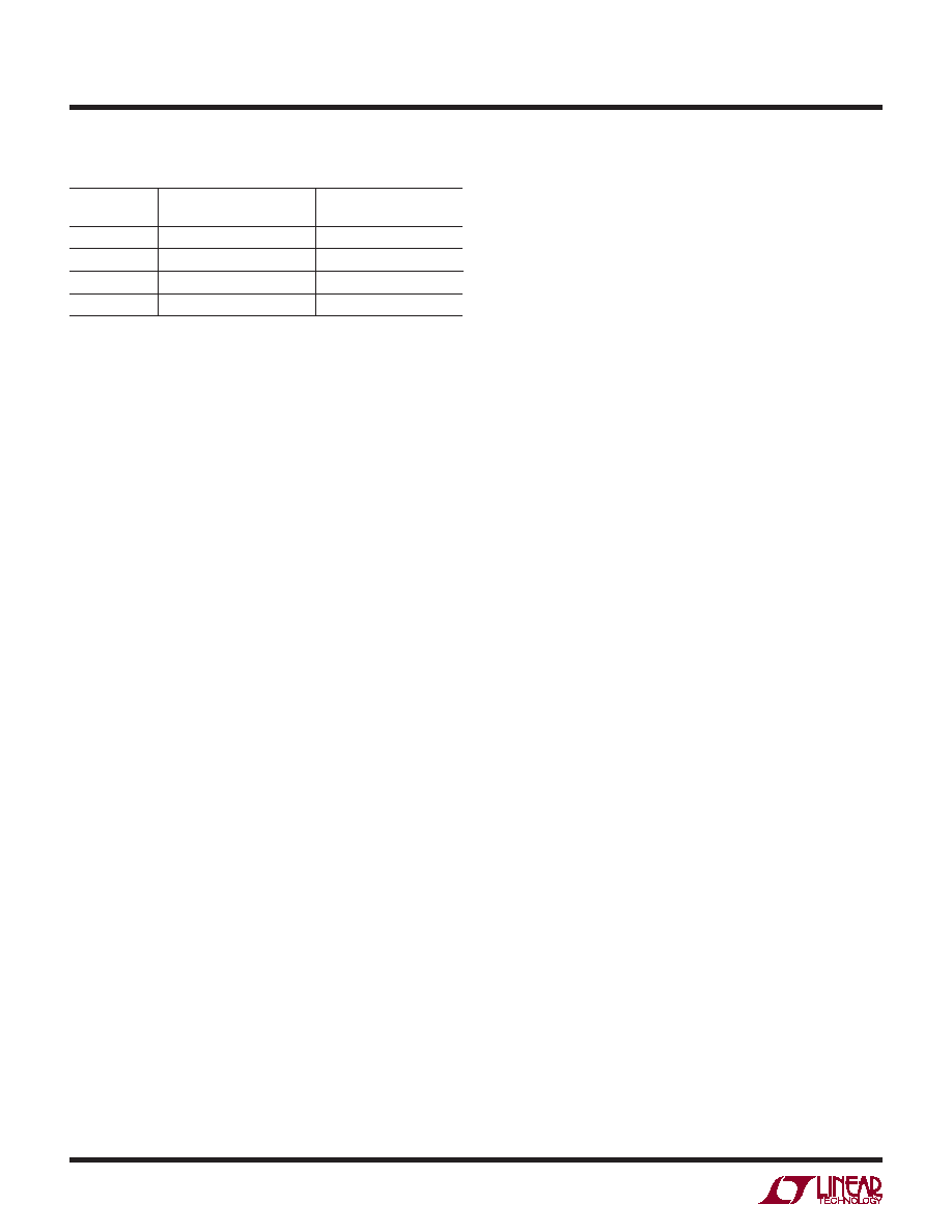
Table 2. MODE Pin Function
MODE PIN
OUTPUT FORMAT
CLOCK DUTY
CYCLE STABILIZER
0
Offset Binary
Off
1/3VDD
Offset Binary
On
2/3VDD
2’s Complement
On
VDD
2’s Complement
Off
Overow Bit
When OF outputs a logic high the converter is either
overranged or underranged on channel A or channel B.
Note that both channels share a common OF pin, which
is not the case for slower pin compatible parts such as
the LTC2284 or LTC2299. OF is disabled when channel A
is in sleep or nap mode.
Output Clock
The ADC has a delayed version of the CLKB input available
as a digital output, CLKOUT. The falling edge of the CLKOUT
pin can be used to latch the digital output data. CLKOUT
is disabled when channel B is in sleep or nap mode.
Output Driver Power
Separate output power and ground pins allow the output
drivers to be isolated from the analog circuitry. The power
supply for the digital output buffers, OVDD, should be tied
to the same power supply as for the logic being driven.
For example, if the converter is driving a DSP powered
by a 1.8V supply, then OVDD should be tied to that same
1.8V supply.
OVDD can be powered with any voltage from 500mV up to
3.6V. OGND can be powered with any voltage from GND
up to 1V and must be less than OVDD. The logic outputs
will swing between OGND and OVDD.
Output Enable
The outputs may be disabled with the output enable pin,
OE. OE high disables all data outputs including OF. The
data access and bus relinquish times are too slow to
allow the outputs to be enabled and disabled during full
speed operation. The output Hi-Z state is intended for use
during long periods of inactivity. Channels A and B have
independent output enable pins (OEA, OEB).
Sleep and Nap Modes
The converter may be placed in shutdown or nap modes
to conserve power. Connecting SHDN to GND results in
normal operation. Connecting SHDN to VDD and OE to VDD
results in sleep mode, which powers down all circuitry
including the reference and typically dissipates 1mW. When
exiting sleep mode it will take milliseconds for the output
data to become valid because the reference capacitors
have to recharge and stabilize. Connecting SHDN to VDD
and OE to GND results in nap mode, which typically dis-
sipates 30mW. In nap mode, the on-chip reference circuit
is kept on, so that recovery from nap mode is faster than
that from sleep mode, typically taking 100 clock cycles. In
both sleep and nap modes, all digital outputs are disabled
and enter the Hi-Z state.
Channels A and B have independent SHDN pins (SHDNA,
SHDNB). Channel A is controlled by SHDNA and OEA,
and channel B is controlled by SHDNB and OEB. The
nap, sleep and output enable modes of the two channels
are completely independent, so it is possible to have one
channel operating while the other channel is in nap or
sleep mode.
Digital Output Multiplexer
The digital outputs of the LTC2285IUP#3CGPBF can be
multiplexed onto a single data bus if the sample rate is
80Msps or less. The MUX pin is a digital input that swaps
the two data busses. If MUX is High, channel A comes
out on DA0-DA13; channel B comes out on DB0-DB13. If
MUX is Low, the output busses are swapped and channel
A comes out on DB0-DB13; channel B comes out on DA0-
DA13. To multiplex both channels onto a single output bus,
connect MUX, CLKA and CLKB together (see the Timing
Diagram for the multiplexed mode). The multiplexed data
is available on either data bus—the unused data bus can
be disabled with its OE pin.
Grounding and Bypassing
The LTC2285IUP#3CGPBF requires a printed circuit board
with a clean, unbroken ground plane. A multilayer board
with an internal ground plane is recommended. Layout
for the printed circuit board should ensure that digital and
analog signal lines are separated as much as possible. In
相关PDF资料 |
PDF描述 |
|---|---|
| LTC2305CDE#PBF | 2-CH 12-BIT SUCCESSIVE APPROXIMATION ADC, SERIAL ACCESS, PDSO12 |
| LTC2305CMS#PBF | 2-CH 12-BIT SUCCESSIVE APPROXIMATION ADC, SERIAL ACCESS, PDSO12 |
| LTC2305IDE#PBF | 2-CH 12-BIT SUCCESSIVE APPROXIMATION ADC, SERIAL ACCESS, PDSO12 |
| LTC2305IDE#TRPBF | 2-CH 12-BIT SUCCESSIVE APPROXIMATION ADC, SERIAL ACCESS, PDSO12 |
| LTC2305IMS#PBF | 2-CH 12-BIT SUCCESSIVE APPROXIMATION ADC, SERIAL ACCESS, PDSO12 |
相关代理商/技术参数 |
参数描述 |
|---|---|
| LTC2285IUPPBF | 制造商:Linear Technology 功能描述:ADC, Dual 14b 125Msps, 3V, LTC2285IUP |
| LTC2285IUP-PBF | 制造商:LINER 制造商全称:Linear Technology 功能描述:Dual 14-Bit, 125Msps Low Power 3V ADC |
| LTC2285IUP-TR | 制造商:LINER 制造商全称:Linear Technology 功能描述:Dual 14-Bit, 125Msps Low Power 3V ADC |
| LTC2285IUP-TRPBF | 制造商:LINER 制造商全称:Linear Technology 功能描述:Dual 14-Bit, 125Msps Low Power 3V ADC |
| LTC2285UP | 制造商:LINER 制造商全称:Linear Technology 功能描述:Dual 14-Bit, 135Msps Low Power 3.3V ADC |
发布紧急采购,3分钟左右您将得到回复。