- 您现在的位置:买卖IC网 > PDF目录39416 > LTC2285IUP#3CGPBF (LINEAR TECHNOLOGY CORP) PROPRIETARY METHOD ADC, PQCC64 PDF资料下载
参数资料
| 型号: | LTC2285IUP#3CGPBF |
| 厂商: | LINEAR TECHNOLOGY CORP |
| 元件分类: | ADC |
| 英文描述: | PROPRIETARY METHOD ADC, PQCC64 |
| 封装: | 9 X 9 MM, LEAD FREE, PLASTIC, QFN-64 |
| 文件页数: | 5/24页 |
| 文件大小: | 578K |
| 代理商: | LTC2285IUP#3CGPBF |
LTC2285IUP#3CGPBF
13
2285iup#3cgpbf
APPLICATIONS INFORMATION
from the input and the held voltage is passed to the ADC
core for processing. As CLK transitions from high to low,
the inputs are reconnected to the sampling capacitors to
acquire a new sample. Since the sampling capacitors still
hold the previous sample, a charging glitch proportional to
the change in voltage between samples will be seen at this
time. If the change between the last sample and the new
sample is small, the charging glitch seen at the input will
be small. If the input change is large, such as the change
seen with input frequencies near Nyquist, then a larger
charging glitch will be seen.
Single-Ended Input
For cost sensitive applications, the analog inputs can be
driven single-ended. With a single-ended input the har-
monic distortion and INL will degrade, but the SNR and
DNL will remain unchanged. For a single-ended input, AIN+
should be driven with the input signal and AIN– should be
connected to 1.5V or VCM.
Common Mode Bias
For optimal performance the analog inputs should be
driven differentially. Each input should swing
±0.5Vforthe
2V range or
±0.25V for the 1V range, around a common
mode voltage of 1.5V. The VCM output pin may be used
to provide the common mode bias level. VCM can be tied
directly to the center tap of a transformer to set the DC
input level or as a reference level to an op amp differential
driver circuit. The VCM pin must be bypassed to ground
close to the ADC with a 2.2μF or greater capacitor.
Input Drive Impedance
As with all high performance, high speed ADCs, the
dynamic performance of the LTC2285IUP#3CGPBF can
be inuenced by the input drive circuitry, particularly the
second and third harmonics. Source impedance and reac-
tance can inuence SFDR. At the falling edge of CLK, the
sample-and-hold circuit will connect the 3.5pF sampling
capacitor to the input pin and start the sampling period.
The sampling period ends when CLK rises, holding the
sampled input on the sampling capacitor. Ideally the input
circuitry should be fast enough to fully charge the sam-
pling capacitor during the sampling period 1/(2FENCODE);
however, this is not always possible and the incomplete
settling may degrade the SFDR. The sampling glitch has
been designed to be as linear as possible to minimize the
effects of incomplete settling.
For the best performance, it is recommended to have a
source impedance of 100Ω or less for each input. The
source impedance should be matched for the differential
inputs. Poor matching will result in higher even order
harmonics, especially the second.
Input Drive Circuits
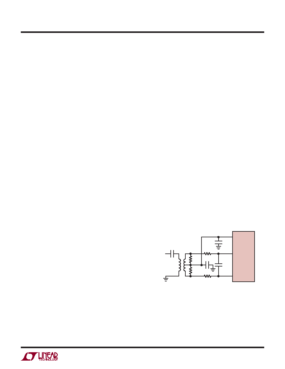
Figure 3 shows the LTC2285IUP#3CGPBF being driven by
an RF transformer with a center tapped secondary. The
secondary center tap is DC biased with VCM, setting the
ADC input signal at its optimum DC level. Terminating on
the transformer secondary is desirable, as this provides
a common mode path for charging glitches caused by
the sample and hold. Figure 3 shows a 1:1 turns ratio
transformer. Other turns ratios can be used if the source
impedance seen by the ADC does not exceed 100Ω for each
ADC input. A disadvantage of using a transformer is the loss
of low frequency response. Most small RF transformers
have poor performance at frequencies below 1MHz.
Figure 3. Single-Ended to Differential
Conversion Using a Transformer
25Ω
0.1μF
AIN
+
AIN
–
12pF
2.2μF
VCM
LTC2285IUP
#3CGPBF
ANALOG
INPUT
0.1μF
T1
1:1
T1 = MA/COM ETC1-1T
RESISTORS, CAPACITORS
ARE 0402 PACKAGE SIZE
2285 F03
相关PDF资料 |
PDF描述 |
|---|---|
| LTC2305CDE#PBF | 2-CH 12-BIT SUCCESSIVE APPROXIMATION ADC, SERIAL ACCESS, PDSO12 |
| LTC2305CMS#PBF | 2-CH 12-BIT SUCCESSIVE APPROXIMATION ADC, SERIAL ACCESS, PDSO12 |
| LTC2305IDE#PBF | 2-CH 12-BIT SUCCESSIVE APPROXIMATION ADC, SERIAL ACCESS, PDSO12 |
| LTC2305IDE#TRPBF | 2-CH 12-BIT SUCCESSIVE APPROXIMATION ADC, SERIAL ACCESS, PDSO12 |
| LTC2305IMS#PBF | 2-CH 12-BIT SUCCESSIVE APPROXIMATION ADC, SERIAL ACCESS, PDSO12 |
相关代理商/技术参数 |
参数描述 |
|---|---|
| LTC2285IUPPBF | 制造商:Linear Technology 功能描述:ADC, Dual 14b 125Msps, 3V, LTC2285IUP |
| LTC2285IUP-PBF | 制造商:LINER 制造商全称:Linear Technology 功能描述:Dual 14-Bit, 125Msps Low Power 3V ADC |
| LTC2285IUP-TR | 制造商:LINER 制造商全称:Linear Technology 功能描述:Dual 14-Bit, 125Msps Low Power 3V ADC |
| LTC2285IUP-TRPBF | 制造商:LINER 制造商全称:Linear Technology 功能描述:Dual 14-Bit, 125Msps Low Power 3V ADC |
| LTC2285UP | 制造商:LINER 制造商全称:Linear Technology 功能描述:Dual 14-Bit, 135Msps Low Power 3.3V ADC |
发布紧急采购,3分钟左右您将得到回复。