- 您现在的位置:买卖IC网 > PDF目录39416 > LTC2285IUP#3CGPBF (LINEAR TECHNOLOGY CORP) PROPRIETARY METHOD ADC, PQCC64 PDF资料下载
参数资料
| 型号: | LTC2285IUP#3CGPBF |
| 厂商: | LINEAR TECHNOLOGY CORP |
| 元件分类: | ADC |
| 英文描述: | PROPRIETARY METHOD ADC, PQCC64 |
| 封装: | 9 X 9 MM, LEAD FREE, PLASTIC, QFN-64 |
| 文件页数: | 24/24页 |
| 文件大小: | 578K |
| 代理商: | LTC2285IUP#3CGPBF |
LTC2285IUP#3CGPBF
9
2285iup#3cgpbf
PIN FUNCTIONS
SHDNA (Pin 59): Channel A Shutdown Mode Selection
Pin. Connecting SHDNA to GND and OEA to GND results
in normal operation with the outputs enabled. Connecting
SHDNA to GND and OEA to VDD results in normal operation
with the outputs at high impedance. Connecting SHDNA
to VDD and OEA to GND results in nap mode with the
outputs at high impedance. Connecting SHDNA to VDD
and OEA to VDD results in sleep mode with the outputs
at high impedance.
MODE (Pin 60): Output Format and Clock Duty Cycle
Stabilizer Selection Pin. Note that MODE controls both
channels. Connecting MODE to GND selects offset binary
output format and turns the clock duty cycle stabilizer
off. 1/3 VDD selects offset binary output format and turns
the clock duty cycle stabilizer on. 2/3 VDD selects 2’s
complement output format and turns the clock duty cycle
stabilizer on. VDD selects 2’s complement output format
and turns the clock duty cycle stabilizer off.
VCMA (Pin 61): Channel A 1.5V Output and Input Common
Mode Bias. Bypass to ground with 2.2μF ceramic chip
capacitor. Do not connect to VCMB.
SENSEA (Pin 62): Channel A Reference Programming Pin.
Connecting SENSEA to VCMA selects the internal reference
and a
±0.5V input range. VDD selects the internal reference
and a
±1V input range. An external reference greater than
0.5V and less than 1V applied to SENSEA selects an input
range of
±VSENSEA. ±1V is the largest valid input range.
GND (Exposed Pad) (Pin 65): ADC Power Ground. The
Exposed Pad on the bottom of the package needs to be
soldered to ground.
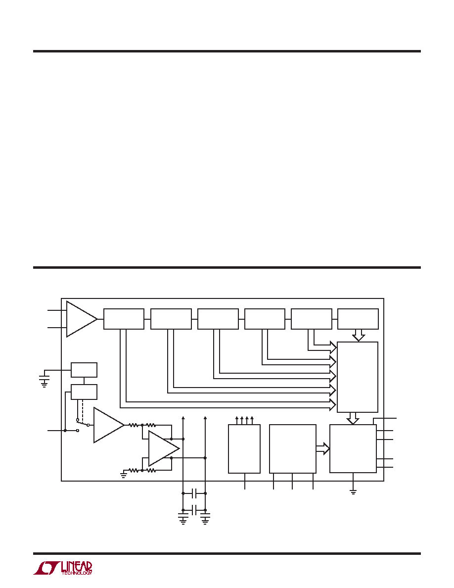
FUNCTIONAL BLOCK DIAGRAM
Figure 1. Functional Block Diagram (Only One Channel is Shown)
SHIFT REGISTER
AND CORRECTION
DIFF
REF
AMP
REF
BUF
2.2μF
1μF
0.1μF
INTERNAL CLOCK SIGNALS
REFH
REFL
CLOCK/DUTY
CYCLE
CONTROL
RANGE
SELECT
1.5V
REFERENCE
FIRST PIPELINED
ADC STAGE
FIFTH PIPELINED
ADC STAGE
SIXTH PIPELINED
ADC STAGE
FOURTH PIPELINED
ADC STAGE
SECOND PIPELINED
ADC STAGE
REFH
REFL
CLK
OE
MODE
OGND
OVDD
2285 F01
INPUT
S/H
SENSE
VCM
AIN
–
AIN
+
2.2μF
THIRD PIPELINED
ADC STAGE
OUTPUT
DRIVERS
CONTROL
LOGIC
SHDN
OF*
D13
D0
CLKOUT*
*OF AND CLKOUT ARE SHARED BETWEEN BOTH CHANNELS.
相关PDF资料 |
PDF描述 |
|---|---|
| LTC2305CDE#PBF | 2-CH 12-BIT SUCCESSIVE APPROXIMATION ADC, SERIAL ACCESS, PDSO12 |
| LTC2305CMS#PBF | 2-CH 12-BIT SUCCESSIVE APPROXIMATION ADC, SERIAL ACCESS, PDSO12 |
| LTC2305IDE#PBF | 2-CH 12-BIT SUCCESSIVE APPROXIMATION ADC, SERIAL ACCESS, PDSO12 |
| LTC2305IDE#TRPBF | 2-CH 12-BIT SUCCESSIVE APPROXIMATION ADC, SERIAL ACCESS, PDSO12 |
| LTC2305IMS#PBF | 2-CH 12-BIT SUCCESSIVE APPROXIMATION ADC, SERIAL ACCESS, PDSO12 |
相关代理商/技术参数 |
参数描述 |
|---|---|
| LTC2285IUPPBF | 制造商:Linear Technology 功能描述:ADC, Dual 14b 125Msps, 3V, LTC2285IUP |
| LTC2285IUP-PBF | 制造商:LINER 制造商全称:Linear Technology 功能描述:Dual 14-Bit, 125Msps Low Power 3V ADC |
| LTC2285IUP-TR | 制造商:LINER 制造商全称:Linear Technology 功能描述:Dual 14-Bit, 125Msps Low Power 3V ADC |
| LTC2285IUP-TRPBF | 制造商:LINER 制造商全称:Linear Technology 功能描述:Dual 14-Bit, 125Msps Low Power 3V ADC |
| LTC2285UP | 制造商:LINER 制造商全称:Linear Technology 功能描述:Dual 14-Bit, 135Msps Low Power 3.3V ADC |
发布紧急采购,3分钟左右您将得到回复。