- 您现在的位置:买卖IC网 > PDF目录10688 > LTC2486IDE#PBF (Linear Technology)IC ADC 16BIT W/PGA 14-DFN PDF资料下载
参数资料
| 型号: | LTC2486IDE#PBF |
| 厂商: | Linear Technology |
| 文件页数: | 8/36页 |
| 文件大小: | 0K |
| 描述: | IC ADC 16BIT W/PGA 14-DFN |
| 标准包装: | 91 |
| 位数: | 16 |
| 采样率(每秒): | 15 |
| 数据接口: | MICROWIRE?,串行,SPI? |
| 转换器数目: | 1 |
| 功率耗散(最大): | 800µW |
| 电压电源: | 单电源 |
| 工作温度: | -40°C ~ 85°C |
| 安装类型: | 表面贴装 |
| 封装/外壳: | 14-WFDFN 裸露焊盘 |
| 供应商设备封装: | 14-DFN-EP(4x3) |
| 包装: | 管件 |
| 输入数目和类型: | 4 个单端,双极;2 个差分,双极 |
| 产品目录页面: | 1348 (CN2011-ZH PDF) |
| 配用: | DC1009A-C-ND - BOARD DELTA SIGMA ADC LTC2486 |
第1页第2页第3页第4页第5页第6页第7页当前第8页第9页第10页第11页第12页第13页第14页第15页第16页第17页第18页第19页第20页第21页第22页第23页第24页第25页第26页第27页第28页第29页第30页第31页第32页第33页第34页第35页第36页
LTC2486
16
2486fd
APPLICATIONS INFORMATION
+FS. If both Bit 21 and Bit 20 are LOW, the differential
input voltage is below –FS. The function of these bits is
summarized in Table 1.
Table 1. LTC2486 Status Bits
Input Range
Bit 23
EOC
Bit 22
DMY
Bit 21
SIG
Bit 20
MSB
VIN ≥ 0.5 VREF/Gain
0011
0V ≤ VIN < 0.5 VREF/Gain
0
1/0
0
–0.5 VREF/Gain ≤ VIN < 0V
0001
VIN < –0.5 VREF/Gain
0000
Bits 20 to 4 are the 16-bit plus sign conversion result
MSB rst.
Bit 4 is the least signicant bit (LSB16).
Bits 3 to 0 are always LOW.
Data is shifted out of the SDO pin under control of the
serial clock (SCK) (see Figure 3). Whenever CS is HIGH,
SDO remains high impedance and SCK is ignored.
In order to shift the conversion result out of the device,
CS must rst be driven LOW. EOC is seen at the SDO pin
of the device once CS is pulled LOW. EOC changes in real
time as a function of the internal oscillator or the clock
applied to the fO pin from HIGH to LOW at the completion
of a conversion. This signal may be used as an interrupt for
an external microcontroller. Bit 23 (EOC) can be captured
on the rst rising edge of SCK. Bit 22 is shifted out of the
device on the rst falling edge of SCK. The nal data bit
(Bit 0) is shifted out on the on the falling edge of the 23rd
SCK and may be latched on the rising edge of the 24th SCK
pulse. On the falling edge of the 24th SCK pulse, SDO goes
HIGH indicating the initiation of a new conversion cycle.
This bit serves as EOC (Bit 23) for the next conversion
cycle. Table 2 summarizes the output data format.
As long as the voltage on the IN+ and IN– pins remains
between –0.3V and VCC + 0.3V (absolute maximum op-
erating range) a conversion result is generated for any
differential input voltage VIN from –FS = –0.5 VREF/Gain
to +FS = 0.5 VREF/Gain. For differential input voltages
greater than +FS, the conversion result is clamped to the
value corresponding to +FS + 1LSB. For differential input
voltages below –FS, the conversion result is clamped to
the value –FS – 1LSB.
INPUT DATA FORMAT
The LTC2486 serial input word is 16 bits long and contains
two distinct sets of data. The rst set (SGL, ODD, A2,
A1, A0) is used to select the input channel. The second
set of data (IM, FA, FB, SPD, GS2, GS1, GS0) is used
to select the frequency rejection, speed mode (1x, 2x),
temperature measurement, and gain.
After power up, the device initiates an internal reset cycle
which sets the input channel to CH0-CH1 (IN+ = CH0, IN– =
CH1), the frequency rejection to simultaneous 50Hz/60Hz,
1x output rate (auto-calibration enabled), and gain = 1. The
rst conversion automatically begins at power up using this
default conguration. Once the conversion is complete, a
new word may be written into the device.
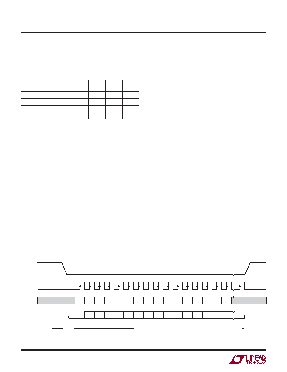
Figure 3. Channel Selection, Conguration Selection and Data Output Timing
EOC
CS
SCK
(EXTERNAL)
SDI
SDO
2486 F03
CONVERSION
SLEEP
DATA INPUT/OUTPUT
MSB
BIT 20 BIT 19 BIT 18 BIT 17 BIT 16 BIT 15 BIT 14 BIT 13 BIT 12 BIT 11
SIG
BIT 21
“0”
BIT 22
BIT 23
1
0
EN
SGL
A2
A1
A0
EN2
IM
FA
FB
SPD
GS2
GS1
GS0
ODD
BIT 10
BIT 9
BIT 0
12
3
4
5
6
7
8
9
10
11
12
13
14
15
16
24
DON'T CARE
相关PDF资料 |
PDF描述 |
|---|---|
| AD8561AR-REEL | IC COMP 7NS ULTRA-FAST 8-SOIC |
| HIN213EIBZ | IC 4DRVR/5RCVR RS232 5V 28-SOIC |
| LTC1444CDHD#PBF | IC COMP QD LP 1.221VREF 16-DFN |
| LTC1445CDHD#PBF | IC COMP QD LP 1.221VREF 16-DFN |
| LTC2487IDE#PBF | IC ADC 16BIT DELTA SIG 14-DFN |
相关代理商/技术参数 |
参数描述 |
|---|---|
| LTC2487CDE#PBF | 功能描述:IC ADC 16BIT DELTA SIG 14-DFN RoHS:是 类别:集成电路 (IC) >> 数据采集 - 模数转换器 系列:- 标准包装:1,000 系列:- 位数:16 采样率(每秒):45k 数据接口:串行 转换器数目:2 功率耗散(最大):315mW 电压电源:模拟和数字 工作温度:0°C ~ 70°C 安装类型:表面贴装 封装/外壳:28-SOIC(0.295",7.50mm 宽) 供应商设备封装:28-SOIC W 包装:带卷 (TR) 输入数目和类型:2 个单端,单极 |
| LTC2487CDE#TRPBF | 功能描述:IC ADC 16BIT DELTA SIG 14-DFN RoHS:是 类别:集成电路 (IC) >> 数据采集 - 模数转换器 系列:- 标准包装:2,500 系列:- 位数:16 采样率(每秒):15 数据接口:MICROWIRE?,串行,SPI? 转换器数目:1 功率耗散(最大):480µW 电压电源:单电源 工作温度:-40°C ~ 85°C 安装类型:表面贴装 封装/外壳:38-WFQFN 裸露焊盘 供应商设备封装:38-QFN(5x7) 包装:带卷 (TR) 输入数目和类型:16 个单端,双极;8 个差分,双极 配用:DC1011A-C-ND - BOARD DELTA SIGMA ADC LTC2494 |
| LTC2487IDE#PBF | 功能描述:IC ADC 16BIT DELTA SIG 14-DFN RoHS:是 类别:集成电路 (IC) >> 数据采集 - 模数转换器 系列:- 标准包装:1 系列:microPOWER™ 位数:8 采样率(每秒):1M 数据接口:串行,SPI? 转换器数目:1 功率耗散(最大):- 电压电源:模拟和数字 工作温度:-40°C ~ 125°C 安装类型:表面贴装 封装/外壳:24-VFQFN 裸露焊盘 供应商设备封装:24-VQFN 裸露焊盘(4x4) 包装:Digi-Reel® 输入数目和类型:8 个单端,单极 产品目录页面:892 (CN2011-ZH PDF) 其它名称:296-25851-6 |
| LTC2487IDE#TRPBF | 功能描述:IC ADC 16BIT DELTA SIG 14-DFN RoHS:是 类别:集成电路 (IC) >> 数据采集 - 模数转换器 系列:- 标准包装:2,500 系列:- 位数:16 采样率(每秒):15 数据接口:MICROWIRE?,串行,SPI? 转换器数目:1 功率耗散(最大):480µW 电压电源:单电源 工作温度:-40°C ~ 85°C 安装类型:表面贴装 封装/外壳:38-WFQFN 裸露焊盘 供应商设备封装:38-QFN(5x7) 包装:带卷 (TR) 输入数目和类型:16 个单端,双极;8 个差分,双极 配用:DC1011A-C-ND - BOARD DELTA SIGMA ADC LTC2494 |
| LTC2488CDE#PBF | 功能描述:IC ADC 16BIT DELTA SIG 14-DFN RoHS:是 类别:集成电路 (IC) >> 数据采集 - 模数转换器 系列:- 标准包装:1 系列:microPOWER™ 位数:8 采样率(每秒):1M 数据接口:串行,SPI? 转换器数目:1 功率耗散(最大):- 电压电源:模拟和数字 工作温度:-40°C ~ 125°C 安装类型:表面贴装 封装/外壳:24-VFQFN 裸露焊盘 供应商设备封装:24-VQFN 裸露焊盘(4x4) 包装:Digi-Reel® 输入数目和类型:8 个单端,单极 产品目录页面:892 (CN2011-ZH PDF) 其它名称:296-25851-6 |
发布紧急采购,3分钟左右您将得到回复。