- 您现在的位置:买卖IC网 > PDF目录98002 > LTC3125EDCB#PBF (LINEAR TECHNOLOGY CORP) SWITCHING REGULATOR, 1900 kHz SWITCHING FREQ-MAX, PDSO8 PDF资料下载
参数资料
| 型号: | LTC3125EDCB#PBF |
| 厂商: | LINEAR TECHNOLOGY CORP |
| 元件分类: | 稳压器 |
| 英文描述: | SWITCHING REGULATOR, 1900 kHz SWITCHING FREQ-MAX, PDSO8 |
| 封装: | 2 X 2 MM, 0.75 MM HEIGHT, LEAD FREE, PLASTIC, DFN-8 |
| 文件页数: | 12/18页 |
| 文件大小: | 303K |
| 代理商: | LTC3125EDCB#PBF |
LTC3125
3
3125fa
Note 1: Stresses beyond those listed under Absolute Maximum Ratings
may cause permanent damage to the device. Exposure to any Absolute
Maximum Rating condition for extended periods may affect device
reliability and lifetime.
Note 2: The LTC3125 is tested under pulsed load conditions such that
TJ ≈ TA. The LTC3125E (E Grade) is guaranteed to meet specications
from 0°C to 85°C junction temperature. Specications over the –40°C
to 125°C operating junction temperature range are assured by design,
characterization and correlation with statistical process controls. The
junction temperature (TJ) is calculated from the ambient temperature
(TA) and power dissipation (PD) according to the formula: TJ = TA + (PD)
(
θJA °C/W), where θJA is the package thermal impedance. The maximum
ambient temperature consistent with these specications is determined by
PARAMETER
CONDITIONS
MIN
TYP
MAX
UNITS
PROG Current Gain
(Note 3)
22.1
kΩ-A/A
Maximum Duty Cycle
VFB = 1.15V
l
85
92
%
Minimum Duty Cycle
VFB = 1.3V
l
0%
Frequency
l
1.3
1.6
1.9
MHz
SHDN Input High
1V
SHDN Input Low
0.35
V
SHDN Input Current
VSHDN = 1.2V
0.3
1
μA
ELECTRICAL CHARACTERISTICS The l denotes the specications which apply over the full operating
junction temperature range, otherwise specications are at TA = 25°C. VIN = 3.3V, VOUT = 4.5V unless otherwise noted (Note 2).
specic operating conditions in conjunction with board layout, the rated
package thermal resistance and other environmental factors.
Note 3: Specication is guaranteed by design and not 100% tested in
production.
Note 4: Current measurements are made when the output is not switching.
Note 5: This IC includes overtemperature protection that is intended
to protect the device during momentary overload conditions. Junction
temperature will exceed 125°C when overtemperature protection is active.
Continuous operation above the specied maximum operating junction
temperature may result in device degradation or failure.
Note 6: Failure to solder the exposed backside of the package to the PC
board ground plane will result in a thermal resistance much higher than
60°C/W.
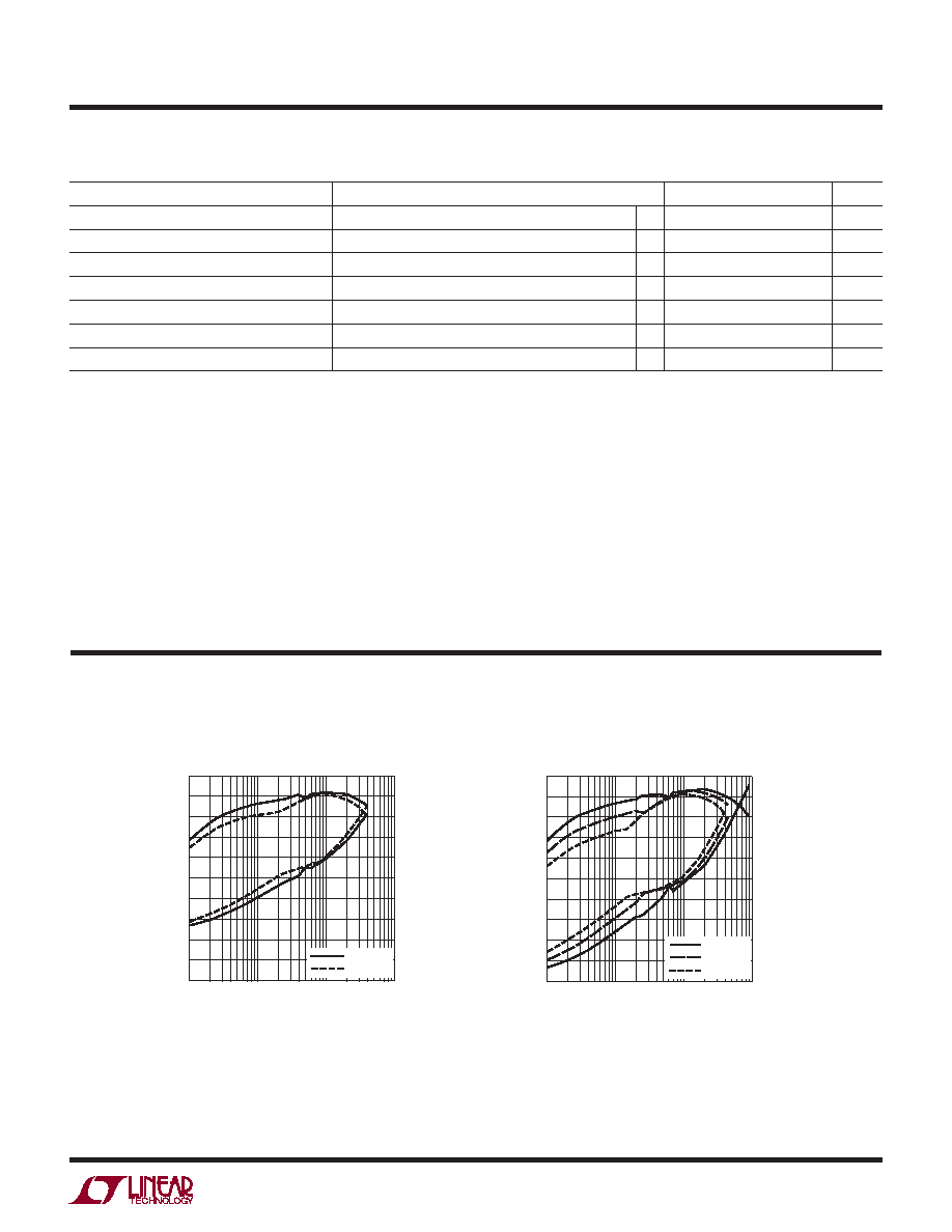
TYPICAL PERFORMANCE CHARACTERISTICS
Efciency vs Load Current,
VOUT = 2.5V
Efciency vs Load Current,
VOUT = 3.3V
(TA = 25°C unless otherwise noted)
LOAD CURRENT (A)
0.001
40
EFFICIENCY
(%)
POWER
LOSS
(W)
50
60
70
80
0.01
0.1
1
3125 G01
30
20
10
0
90
100
0.1
0.01
0.0001
0.001
1
VIN = 2.1V
VIN = 1.8V
LOAD CURRENT (A)
0.001
40
EFFICIENCY
(%)
POWER
LOSS
(W)
50
60
70
80
0.01
0.1
1
3125 G02
30
20
10
0
90
100
0.1
0.01
0.001
1
VIN = 2.8V
VIN = 2.4V
VIN = 2V
相关PDF资料 |
PDF描述 |
|---|---|
| LTC3406ES5-1.2#PBF | 1.3 A SWITCHING REGULATOR, 1800 kHz SWITCHING FREQ-MAX, PDSO5 |
| LTC3414MPFE#PBF | 9.5 A SWITCHING REGULATOR, 4000 kHz SWITCHING FREQ-MAX, PDSO20 |
| LTC3522EUD#TR | 0.85 A DUAL SWITCHING CONTROLLER, 1330 kHz SWITCHING FREQ-MAX, PQCC16 |
| LTC3525LESC6-3#PBF | 0.45 A SWITCHING REGULATOR, PDSO6 |
| LTC3526LEDC | SWITCHING CONTROLLER, 1250 kHz SWITCHING FREQ-MAX, PDSO6 |
相关代理商/技术参数 |
参数描述 |
|---|---|
| LTC3125EDCBTRMPBF | 制造商:Linear Technology 功能描述:DC-DC Converter Step-Up 1.8-5.5V DFN8EP |
| LTC3125EDCB-TRPBF | 制造商:LINER 制造商全称:Linear Technology 功能描述:1.2A Synchronous Step-Up DC/DC Converter with Input Current Limit |
| LTC3127 | 制造商:LINEAR 制造商全称:LINEAR 功能描述:40V, 2A Synchronous Buck-Boost DC/DC Converter |
| LTC3127EDD | 制造商:LINER 制造商全称:Linear Technology 功能描述:1A Buck-Boost DC/DC Converter with Programmable Input Current Limit |
| LTC3127EDD#PBF | 功能描述:IC BUCK BOOST SYNC ADJ 10DFN RoHS:是 类别:集成电路 (IC) >> PMIC - 电源管理 - 专用 系列:- 产品培训模块:Lead (SnPb) Finish for COTS Obsolescence Mitigation Program 标准包装:50 系列:- 应用:热电冷却器 电流 - 电源:- 电源电压:3 V ~ 5.5 V 工作温度:-40°C ~ 85°C 安装类型:表面贴装 封装/外壳:28-SOIC(0.173",4.40mm 宽)裸露焊盘 供应商设备封装:28-TSSOP 裸露焊盘 包装:管件 产品目录页面:1410 (CN2011-ZH PDF) |
发布紧急采购,3分钟左右您将得到回复。