- 您现在的位置:买卖IC网 > PDF目录98002 > LTC3125EDCB#PBF (LINEAR TECHNOLOGY CORP) SWITCHING REGULATOR, 1900 kHz SWITCHING FREQ-MAX, PDSO8 PDF资料下载
参数资料
| 型号: | LTC3125EDCB#PBF |
| 厂商: | LINEAR TECHNOLOGY CORP |
| 元件分类: | 稳压器 |
| 英文描述: | SWITCHING REGULATOR, 1900 kHz SWITCHING FREQ-MAX, PDSO8 |
| 封装: | 2 X 2 MM, 0.75 MM HEIGHT, LEAD FREE, PLASTIC, DFN-8 |
| 文件页数: | 15/18页 |
| 文件大小: | 303K |
| 代理商: | LTC3125EDCB#PBF |
LTC3125
6
3125fa
PIN FUNCTIONS
GND (Pin 1, Exposed Pad Pin 9): Ground. The exposed
pad must be soldered to the PCB ground plane for electrical
connection and for rated thermal performance.
FB (Pin 2): Feedback Input to the Error Amplier. Connect
the resistor divider tap to this pin. The top of the divider
connects to VOUT and the bottom of the divider connects
to GND. The output voltage can be adjusted from 1.8V
to 5.25V.
PROG (Pin 3): Programming Input for Average Input Cur-
rent. This pin should be connected to ground through an
external resistor (RPROG) to set input average current limit
threshold. Refer to the Component Selection section in
Applications Information for details on selecting RPROG.
VIN (Pin 4): Input Voltage. The device is powered from VIN
until VOUT exceeds VIN. Once VOUT is greater than (VIN +
0.25V), the device is powered from VOUT. Place a ceramic
bypass capacitor from VIN to GND. A minimum value of
1μF is recommended. Also connects to CS through 60mΩ
internal sense resistor.
CS (Pin 5): Current Sense Resistor Connection Point.
Connect the inductor directly to CS. An internal 60mΩ
sense resistor is connected between CS and VIN.
SHDN (Pin 6): Logic Controlled Shutdown Input. Bringing
this pin above 1V enables the part, forcing this pin below
0.35V disables the part.
VOUT (Pin 7): Output Voltage Sense and the Output of the
Synchronous Rectier. Connect the output lter capacitor
from VOUT to GND, close to the IC. A minimum value of
150μF is recommended. Due to the output disconnect
feature, VOUT is disconnected from VIN when SHDN is low.
SW (Pin 8): Switch Pin. Connect an inductor from this
pin to CS. An internal anti-ringing resistor is connected
across SW and CS after the inductor current has dropped
near zero.
TYPICAL PERFORMANCE CHARACTERISTICS (T
A = 25°C unless otherwise noted)
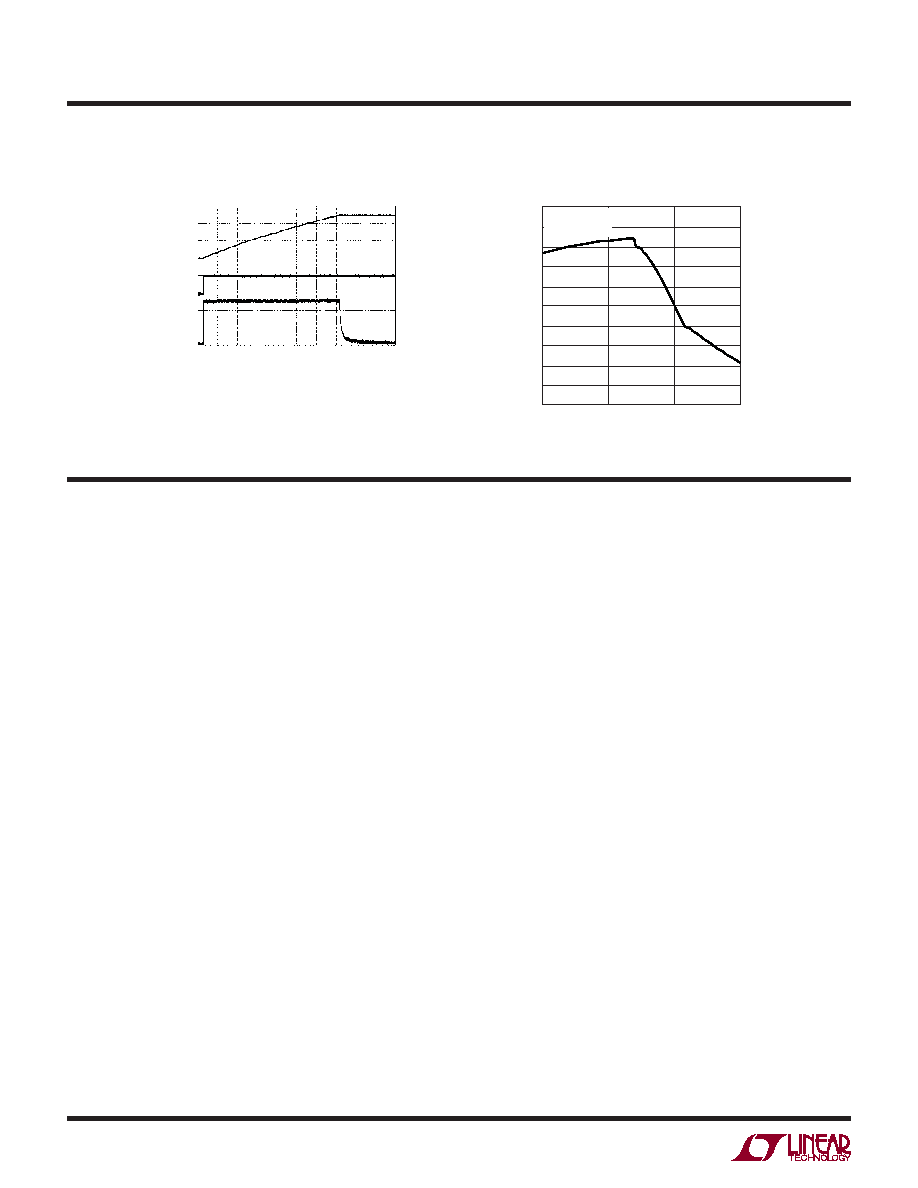
VOUT and IIN During Soft-Start
VOUT
2V/DIV
SHDN
5V/DIV
INPUT
CURRENT
200mA/DIV
2s/DIV
VIN = 3.3V
VOUT = 4.5V
COUT = 1F
L = 2.7μH
3125 G20
Efciency vs VIN
VIN (V)
2
50
EFFICIENCY
(%)
60
65
70
75
80
85
3
4
3125 G21
90
95
100
55
5
ILOAD = 200mA
VOUT = 3.8V
相关PDF资料 |
PDF描述 |
|---|---|
| LTC3406ES5-1.2#PBF | 1.3 A SWITCHING REGULATOR, 1800 kHz SWITCHING FREQ-MAX, PDSO5 |
| LTC3414MPFE#PBF | 9.5 A SWITCHING REGULATOR, 4000 kHz SWITCHING FREQ-MAX, PDSO20 |
| LTC3522EUD#TR | 0.85 A DUAL SWITCHING CONTROLLER, 1330 kHz SWITCHING FREQ-MAX, PQCC16 |
| LTC3525LESC6-3#PBF | 0.45 A SWITCHING REGULATOR, PDSO6 |
| LTC3526LEDC | SWITCHING CONTROLLER, 1250 kHz SWITCHING FREQ-MAX, PDSO6 |
相关代理商/技术参数 |
参数描述 |
|---|---|
| LTC3125EDCBTRMPBF | 制造商:Linear Technology 功能描述:DC-DC Converter Step-Up 1.8-5.5V DFN8EP |
| LTC3125EDCB-TRPBF | 制造商:LINER 制造商全称:Linear Technology 功能描述:1.2A Synchronous Step-Up DC/DC Converter with Input Current Limit |
| LTC3127 | 制造商:LINEAR 制造商全称:LINEAR 功能描述:40V, 2A Synchronous Buck-Boost DC/DC Converter |
| LTC3127EDD | 制造商:LINER 制造商全称:Linear Technology 功能描述:1A Buck-Boost DC/DC Converter with Programmable Input Current Limit |
| LTC3127EDD#PBF | 功能描述:IC BUCK BOOST SYNC ADJ 10DFN RoHS:是 类别:集成电路 (IC) >> PMIC - 电源管理 - 专用 系列:- 产品培训模块:Lead (SnPb) Finish for COTS Obsolescence Mitigation Program 标准包装:50 系列:- 应用:热电冷却器 电流 - 电源:- 电源电压:3 V ~ 5.5 V 工作温度:-40°C ~ 85°C 安装类型:表面贴装 封装/外壳:28-SOIC(0.173",4.40mm 宽)裸露焊盘 供应商设备封装:28-TSSOP 裸露焊盘 包装:管件 产品目录页面:1410 (CN2011-ZH PDF) |
发布紧急采购,3分钟左右您将得到回复。