- 您现在的位置:买卖IC网 > PDF目录1829 > LTC3404MPMS8#PBF (Linear Technology)IC REG BUCK SYNC ADJ 0.6A 8MSOP PDF资料下载
参数资料
| 型号: | LTC3404MPMS8#PBF |
| 厂商: | Linear Technology |
| 文件页数: | 12/16页 |
| 文件大小: | 0K |
| 描述: | IC REG BUCK SYNC ADJ 0.6A 8MSOP |
| 标准包装: | 50 |
| 类型: | 降压(降压) |
| 输出类型: | 可调式 |
| 输出数: | 1 |
| 输出电压: | 0.8 V ~ 6 V |
| 输入电压: | 2.65 V ~ 6 V |
| PWM 型: | 电流模式,混合 |
| 频率 - 开关: | 1.4MHz |
| 电流 - 输出: | 600mA |
| 同步整流器: | 是 |
| 工作温度: | -55°C ~ 125°C |
| 安装类型: | 表面贴装 |
| 封装/外壳: | 8-TSSOP,8-MSOP(0.118",3.00mm 宽) |
| 包装: | 管件 |
| 供应商设备封装: | 8-MSOP |
�� �
�
�LTC3404�
�APPLICATIO� S� I� FOR� ATIO�
�very� low� load� currents� can� be� misleading� since� the� actual�
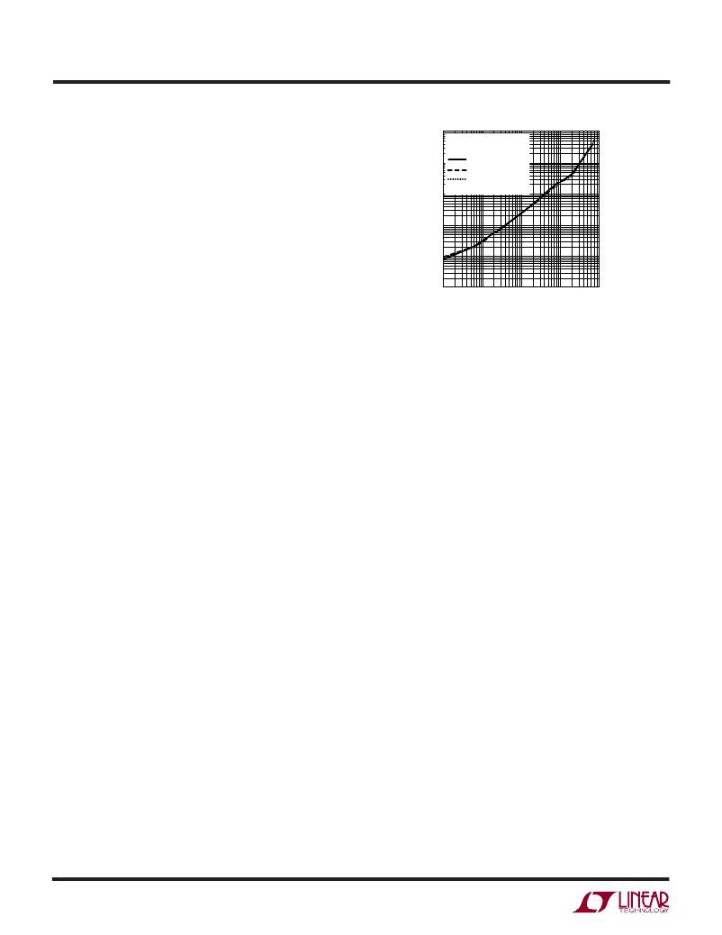
�power� lost� is� of� no� consequence� as� illustrated� in� Figure� 6.�
�1.� The� V� IN� quiescent� current� is� due� to� two� components:�
�the� DC� bias� current� as� given� in� the� electrical� character-�
�istics� and� the� internal� main� switch� and� synchronous�
�switch� gate� charge� currents.� The� gate� charge� current�
�results� from� switching� the� gate� capacitance� of� the�
�internal� power� MOSFET� switches.� Each� time� the� gate� is�
�switched� from� high� to� low� to� high� again,� a� packet� of�
�1�
�0.1�
�0.01�
�0.001�
�0.0001�
�V� IN� =� 4.2V�
�L� =� 4.7� μ� H�
�V� OUT� =� 1.5V�
�V� OUT� =� 2.5V�
�V� OUT� =� 3.3V�
�Burst� Mode� OPERATION�
�charge� dQ� moves� from� V� IN� to� ground.� The� resulting�
�0.00001�
�0.1�
�1�
�10� 100�
�1000�
�dQ/dt� is� the� current� out� of� V� IN� that� is� typically� larger� than�
�the� DC� bias� current.� In� continuous� mode,� I� GATECHG� =�
�f(Q� T� +� Q� B� )� where� Q� T� and� Q� B� are� the� gate� charges� of� the�
�internal� top� and� bottom� switches.� Both� the� DC� bias� and�
�gate� charge� losses� are� proportional� to� V� IN� and� thus�
�their� effects� will� be� more� pronounced� at� higher� supply�
�voltages.�
�2.� I� 2� R� losses� are� calculated� from� the� resistances� of� the�
�internal� switches,� R� SW� ,� and� external� inductor� R� L� .� In�
�continuous� mode� the� average� output� current� flowing�
�through� inductor� L� is� “chopped”� between� the� main�
�switch� and� the� synchronous� switch.� Thus,� the� series�
�resistance� looking� into� the� SW� pin� is� a� function� of� both�
�top� and� bottom� MOSFET� R� DS(ON)� and� the� duty� cycle�
�(DC)� as� follows:�
�R� SW� =� (R� DS(ON)TOP� )(DC)� +� (R� DS(ON)BOT� )(1� –� DC)�
�The� R� DS(ON)� for� both� the� top� and� bottom� MOSFETs� can�
�be� obtained� from� the� Typical� Performance� Charateristics�
�curves.� Thus,� to� obtain� I� 2� R� losses,� simply� add� R� SW� to�
�R� L� and� multiply� the� result� by� the� square� of� the� average�
�output� current.�
�Other� losses� including� C� IN� and� C� OUT� ESR� dissipative�
�losses� and� inductor� core� losses� generally� account� for� less�
�than� 2%� total� additional� loss.�
�Thermal� Considerations�
�In� most� applications� the� LTC3404� does� not� dissipate�
�much� heat� due� to� its� high� efficiency.� But,� in� applications�
�where� the� LTC3404� is� running� at� high� ambient� tempera-�
�ture� with� low� supply� voltage� and� high� duty� cycles,� such�
�as� in� dropout,� the� heat� dissipated� may� exceed� the� maxi-�
�mum� junction� temperature� of� the� part.� If� the� junction�
�LOAD� CURRENT� (mA)�
�3404� F06�
�Figure� 6.� Power� Lost� vs� Load� Current�
�temperature� reaches� approximately� 175� °� C,� both� power�
�switches� will� be� turned� off� and� the� SW� node� will� become�
�high� impedance.�
�To� avoid� the� LTC3404� from� exceeding� the� maximum�
�junction� temperature,� the� user� will� need� to� do� some�
�thermal� analysis.� The� goal� of� the� thermal� analysis� is� to�
�determine� whether� the� power� dissipated� exceeds� the�
�maximum� junction� temperature� of� the� part.� The� tempera-�
�ture� rise� is� given� by:�
�T� R� =� (P� D� )(� θ� JA� )�
�where� P� D� is� the� power� dissipated� by� the� regulator� and� q� JA�
�is� the� thermal� resistance� from� the� junction� of� the� die� to� the�
�ambient� temperature.�
�The� junction� temperature,� T� J� ,� is� given� by:�
�T� J� =� T� A� +� T� R�
�where� T� A� is� the� ambient� temperature.�
�As� an� example,� consider� the� LTC3404� in� dropout� at� an�
�input� voltage� of� 3V,� a� load� current� of� 500mA,� and� an�
�ambient� temperature� of� 70� °� C.� From� the� typical� perfor-�
�mance� graph� of� switch� resistance,� the� R� DS(ON)� of� the�
�P-channel� switch� at� 70� °� C� is� approximately� 0.7� Ω� .� There-�
�fore,� power� dissipated� by� the� part� is:�
�P� D� =� I� LOAD2� ?� R� DS(ON)� =� 0.175W�
�For� the� MSOP� package,� the� θ� JA� is� 150� °� C/� W.� Thus,� the�
�junction� temperature� of� the� regulator� is:�
�T� J� =� 70� °� C� +� (0.175)(150)� =� 96� °� C�
�3404fb�
�12�
�相关PDF资料 |
PDF描述 |
|---|---|
| LTC3405ES6#TRPBF | IC REG BUCK SYNC ADJ .3A SOT23-6 |
| LTC3406BES5-1.2#TRPBF | IC REG BUCK SYNC 1.2V TSOT23-5 |
| LTC3406ES5-1.8#TRPBF | IC REG BUCK SYNC 1.8V TSOT23-5 |
| LTC3407EDD#TRPBF | IC REG BUCK SYNC ADJ 1A DL 10DFN |
| LTC3408EDD#TRPBF | IC REG BUCK W/BYPASS TXRX 8-DFN |
相关代理商/技术参数 |
参数描述 |
|---|---|
| LTC3405 | 制造商:LINEAR 制造商全称:LINEAR 功能描述:Standalone 250mA Li-Ion Battery Charger in 2 × 2 DFN |
| LTC3405A | 制造商:LINER 制造商全称:Linear Technology 功能描述:1.5MHz, 300mA Synchronous Step-Down Regulator in ThinSOT |
| LTC3405A-1.375 | 制造商:LINER 制造商全称:Linear Technology 功能描述:1.375V, 1.5MHz, 300mA Synchronous Step-Down Regulators in ThinSOT |
| LTC3405A-1.5 | 制造商:LINER 制造商全称:Linear Technology 功能描述:1.5V, 1.8V, 1.5MHz, 300mA Synchronous Step-Down Regulators in ThinSOT |
| LTC3405A-1.8 | 制造商:LINER 制造商全称:Linear Technology 功能描述:1.5V, 1.8V, 1.5MHz, 300mA Synchronous Step-Down Regulators in ThinSOT |
发布紧急采购,3分钟左右您将得到回复。