- 您现在的位置:买卖IC网 > PDF目录1829 > LTC3404MPMS8#PBF (Linear Technology)IC REG BUCK SYNC ADJ 0.6A 8MSOP PDF资料下载
参数资料
| 型号: | LTC3404MPMS8#PBF |
| 厂商: | Linear Technology |
| 文件页数: | 7/16页 |
| 文件大小: | 0K |
| 描述: | IC REG BUCK SYNC ADJ 0.6A 8MSOP |
| 标准包装: | 50 |
| 类型: | 降压(降压) |
| 输出类型: | 可调式 |
| 输出数: | 1 |
| 输出电压: | 0.8 V ~ 6 V |
| 输入电压: | 2.65 V ~ 6 V |
| PWM 型: | 电流模式,混合 |
| 频率 - 开关: | 1.4MHz |
| 电流 - 输出: | 600mA |
| 同步整流器: | 是 |
| 工作温度: | -55°C ~ 125°C |
| 安装类型: | 表面贴装 |
| 封装/外壳: | 8-TSSOP,8-MSOP(0.118",3.00mm 宽) |
| 包装: | 管件 |
| 供应商设备封装: | 8-MSOP |
�� �
�
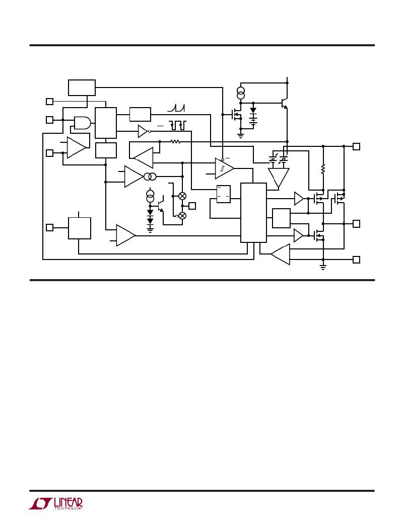
�LTC3404�
�FU� CTIO� AL� DIAGRA�
�V� IN�
�PLL� LPF�
�BURST�
�DEFEAT�
�X�
�Y�
�Y� =� “0”� ONLY� WHEN� X� IS� A� CONSTANT� “1”�
�8�
�SYNC/MODE�
�7�
�VCO�
�SLOPE�
�COMP�
�0.8V�
�OSC�
�3�
�0.6V�
�–�
�+�
�FREQ�
�SHIFT�
�–�
�6� V� IN�
�V� FB�
�V� REF�
�0.8V�
�EA�
�+�
�V� IN� SLEEP�
�0.55V�
�–�
�+�
�EN�
�BURST�
�SLEEP�
�–� +�
�I� COMP�
�6� Ω�
�g� m� =� 0.5m�
�V� IN�
�S�
�R�
�Q�
�Q�
�V� IN�
�2� I� TH�
�RS� LATCH�
�SWITCHING�
�LOGIC�
�P-CH�
�P-CH�
�AND�
�ANTI-�
�RUN�
�1�
�0.8V� REF�
�–�
�BLANKING�
�CIRCUIT�
�SHOOT-�
�THRU�
�5� SW�
�OVDET�
�0.85V�
�+�
�N-CH�
�SHUTDOWN�
�I� RCMP�
�4� GND�
�3404� BD�
�OPERATIO�
�Main� Control� Loop�
�The� LTC3404� uses� a� constant� frequency,� current� mode�
�step-down� architecture.� Both� the� main� (P-channel� MOS-�
�FET)� and� synchronous� (N-channel� MOSFET)� switches� are�
�internal.� During� normal� operation,� the� internal� top� power�
�MOSFET� is� turned� on� each� clock� cycle� when� the� oscillator�
�sets� the� RS� latch,� and� turned� off� when� the� current� com-�
�parator,� I� COMP� ,� resets� the� RS� latch.� The� peak� inductor�
�current� at� which� I� COMP� resets� the� RS� latch� is� controlled� by�
�the� voltage� on� the� I� TH� pin,� which� is� the� output� of� error�
�amplifier� EA.� The� V� FB� pin,� described� in� the� Pin� Functions�
�section,� allows� EA� to� receive� an� output� feedback� voltage�
�from� an� external� resistive� divider.� When� the� load� current�
�increases,� it� causes� a� slight� decrease� in� the� feedback�
�voltage,� V� FB� ,� relative� to� the� 0.8V� internal� reference,� which�
�in� turn,� causes� the� I� TH� voltage� to� increase� until� the� average�
�inductor� current� matches� the� new� load� current.� While� the�
�top� MOSFET� is� off,� the� bottom� MOSFET� is� turned� on� until�
�either� the� inductor� current� starts� to� reverse� as� indicated� by�
�the� current� reversal� comparator� I� RCMP� ,� or� the� beginning� of�
�the� next� clock� cycle.�
�Comparator� OVDET� guards� against� transient� overshoots�
�>6.25%� by� turning� the� main� switch� off� and� keeping� it� off�
�until� the� fault� is� removed.�
�Burst� Mode� Operation�
�The� LTC3404� is� capable� of� Burst� Mode� operation� in� which�
�the� internal� power� MOSFETs� operate� intermittently� based�
�on� load� demand.� To� enable� Burst� Mode� operation,� simply�
�tie� the� SYNC/MODE� pin� to� V� IN� or� connect� it� to� a� logic� high�
�(V� SYNC/MODE� >� 1.5V).� To� disable� Burst� Mode� operation� and�
�enable� PWM� pulse� skipping� mode,� connect� the� SYNC/�
�MODE� pin� to� GND.� In� this� mode,� the� efficiency� is� lower� at�
�light� loads,� but� becomes� comparable� to� Burst� Mode�
�operation� when� the� output� load� exceeds� 50mA.� The� ad-�
�vantage� of� pulse� skipping� mode� is� lower� output� ripple� and�
�less� interference� to� audio� circuitry.�
�3404fb�
�7�
�相关PDF资料 |
PDF描述 |
|---|---|
| LTC3405ES6#TRPBF | IC REG BUCK SYNC ADJ .3A SOT23-6 |
| LTC3406BES5-1.2#TRPBF | IC REG BUCK SYNC 1.2V TSOT23-5 |
| LTC3406ES5-1.8#TRPBF | IC REG BUCK SYNC 1.8V TSOT23-5 |
| LTC3407EDD#TRPBF | IC REG BUCK SYNC ADJ 1A DL 10DFN |
| LTC3408EDD#TRPBF | IC REG BUCK W/BYPASS TXRX 8-DFN |
相关代理商/技术参数 |
参数描述 |
|---|---|
| LTC3405 | 制造商:LINEAR 制造商全称:LINEAR 功能描述:Standalone 250mA Li-Ion Battery Charger in 2 × 2 DFN |
| LTC3405A | 制造商:LINER 制造商全称:Linear Technology 功能描述:1.5MHz, 300mA Synchronous Step-Down Regulator in ThinSOT |
| LTC3405A-1.375 | 制造商:LINER 制造商全称:Linear Technology 功能描述:1.375V, 1.5MHz, 300mA Synchronous Step-Down Regulators in ThinSOT |
| LTC3405A-1.5 | 制造商:LINER 制造商全称:Linear Technology 功能描述:1.5V, 1.8V, 1.5MHz, 300mA Synchronous Step-Down Regulators in ThinSOT |
| LTC3405A-1.8 | 制造商:LINER 制造商全称:Linear Technology 功能描述:1.5V, 1.8V, 1.5MHz, 300mA Synchronous Step-Down Regulators in ThinSOT |
发布紧急采购,3分钟左右您将得到回复。