- 您现在的位置:买卖IC网 > PDF目录1829 > LTC3404MPMS8#PBF (Linear Technology)IC REG BUCK SYNC ADJ 0.6A 8MSOP PDF资料下载
参数资料
| 型号: | LTC3404MPMS8#PBF |
| 厂商: | Linear Technology |
| 文件页数: | 13/16页 |
| 文件大小: | 0K |
| 描述: | IC REG BUCK SYNC ADJ 0.6A 8MSOP |
| 标准包装: | 50 |
| 类型: | 降压(降压) |
| 输出类型: | 可调式 |
| 输出数: | 1 |
| 输出电压: | 0.8 V ~ 6 V |
| 输入电压: | 2.65 V ~ 6 V |
| PWM 型: | 电流模式,混合 |
| 频率 - 开关: | 1.4MHz |
| 电流 - 输出: | 600mA |
| 同步整流器: | 是 |
| 工作温度: | -55°C ~ 125°C |
| 安装类型: | 表面贴装 |
| 封装/外壳: | 8-TSSOP,8-MSOP(0.118",3.00mm 宽) |
| 包装: | 管件 |
| 供应商设备封装: | 8-MSOP |
�� �
�
�LTC3404�
�APPLICATIO� S� I� FOR� ATIO�
�which� is� below� the� maximum� junction� temperature� of�
�125� °� C.�
�Note� that� at� higher� supply� voltages,� the� junction� tempera-�
�ture� is� lower� due� to� reduced� switch� resistance� (R� DS(ON)� ).�
�Checking� Transient� Response�
�The� regulator� loop� response� can� be� checked� by� looking� at�
�the� load� transient� response.� Switching� regulators� take�
�several� cycles� to� respond� to� a� step� in� load� current.� When�
�a� load� step� occurs,� V� OUT� immediately� shifts� by� an� amount�
�equal� to� (� Δ� I� LOAD� ?� ESR),� where� ESR� is� the� effective� series�
�resistance� of� C� OUT� .� Δ� I� LOAD� also� begins� to� charge� or�
�discharge� C� OUT� ,� which� generates� a� feedback� error� signal.�
�The� regulator� loop� then� acts� to� return� V� OUT� to� its� steady-�
�state� value.� During� this� recovery� time� V� OUT� can� be� moni-�
�tored� for� overshoot� or� ringing� that� would� indicate� a� stabil-�
�ity� problem.� The� internal� compensation� provides� adequate�
�compensation� for� most� applications.� But� if� additional�
�compensation� is� required,� the� I� TH� pin� can� be� used� for�
�external� compensation� using� R� C� ,� C� C1� as� shown� in�
�Figure� 7.� (The� 47pF� capacitor,� C� C2� ,� is� typically� needed� for�
�noise� decoupling.)�
�A� second,� more� severe� transient� is� caused� by� switching� in�
�loads� with� large� (>1� μ� F)� supply� bypass� capacitors.� The�
�discharged� bypass� capacitors� are� effectively� put� in� parallel�
�with� C� OUT� ,� causing� a� rapid� drop� in� V� OUT� .� No� regulator� can�
�deliver� enough� current� to� prevent� this� problem� if� the� load�
�switch� resistance� is� low� and� it� is� driven� quickly.� The� only�
�solution� is� to� limit� the� rise� time� of� the� switch� drive� so� that�
�the� load� rise� time� is� limited� to� approximately� (25� ?� C� LOAD� ).�
�C� C2�
�Thus,� a� 10� μ� F� capacitor� charging� to� 3.3V� would� require� a�
�250� μ� s� rise� time,� limiting� the� charging� current� to� about�
�130mA.�
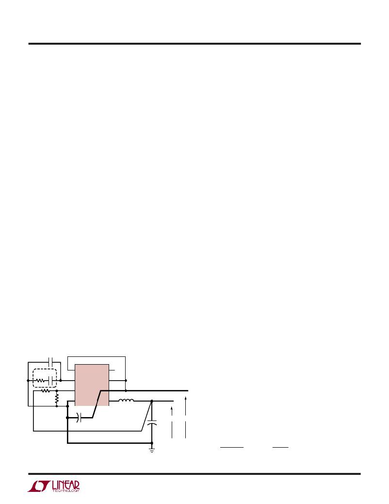
�PC� Board� Layout� Checklist�
�When� laying� out� the� printed� circuit� board,� the� following�
�checklist� should� be� used� to� ensure� proper� operation� of� the�
�LTC3404.� These� items� are� also� illustrated� graphically� in�
�the� layout� diagram� of� Figure� 7.� Check� the� following� in� your�
�layout:�
�1.� Are� the� signal� and� power� grounds� segregated?� The�
�LTC3404� signal� ground� consists� of� the� resistive�
�divider,� the� optional� compensation� network� (R� C� and�
�C� C1� )� and� C� C2� .� The� power� ground� consists� of� the� (–)�
�plate� of� C� IN� ,� the� (–)� plate� of� C� OUT� and� Pin� 4� of� the�
�LTC3404.� The� power� ground� traces� should� be� kept�
�short,� direct� and� wide.� The� signal� ground� and� power�
�ground� should� converge� to� a� common� node� in� a� star-�
�ground� configuration.�
�2.� Does� the� V� FB� pin� connect� directly� to� the� feedback�
�resistors?� The� resistive� divider� R1/R2� must� be� con-�
�nected� between� the� (+)� plate� of� C� OUT� and� signal� ground.�
�3.� Does� the� (+)� plate� of� C� IN� connect� to� V� IN� as� closely� as�
�possible?� This� capacitor� provides� the� AC� current� to� the�
�internal� power� MOSFETs.�
�4.� Keep� the� switching� node� SW� away� from� sensitive� small�
�signal� nodes.�
�Design� Example�
�As� a� design� example,� assume� the� LTC3404� is� used� in� a�
�OPTIONAL�
�R� C�
�R2�
�C� C1�
�R1�
�1�
�2�
�3�
�4�
�LTC3404�
�RUN� PLL� LPF�
�I� TH� SYNC/MODE�
�V� FB�
�GND� SW�
�C� IN�
�+�
�8�
�7�
�V� IN� 6�
�5�
�L1�
�BOLD� LINES� INDICATE�
�HIGH� CURRENT� PATHS�
�+�
�+� V� OUT�
�C� OUT�
�+�
�V� IN�
�single� lithium-ion� battery-powered� cellular� phone� applica-�
�tion.� The� input� voltage� will� be� operating� from� a� maximum�
�of� 4.2V� down� to� about� 2.7V.� The� load� current� requirement�
�is� a� maximum� of� 0.3A� but� most� of� the� time� it� will� be� in�
�standby� mode,� requiring� only� 2mA.� Efficiency� at� both� low�
�and� high� load� currents� is� important.� Output� voltage� is�
�2.5V.� With� this� information� we� can� calculate� L� using�
�equation� (1),�
�V� OUT� ?� 1� ?� OUT� ?�
�–�
�–�
�3404� F07�
�L� =�
�1�
�(� )� f� (� Δ� I� L� )�
�?� V� ?�
�?� V� IN� ?�
�(3)�
�Figure� 7.� LTC3404� Layout� Diagram�
�3404fb�
�13�
�相关PDF资料 |
PDF描述 |
|---|---|
| LTC3405ES6#TRPBF | IC REG BUCK SYNC ADJ .3A SOT23-6 |
| LTC3406BES5-1.2#TRPBF | IC REG BUCK SYNC 1.2V TSOT23-5 |
| LTC3406ES5-1.8#TRPBF | IC REG BUCK SYNC 1.8V TSOT23-5 |
| LTC3407EDD#TRPBF | IC REG BUCK SYNC ADJ 1A DL 10DFN |
| LTC3408EDD#TRPBF | IC REG BUCK W/BYPASS TXRX 8-DFN |
相关代理商/技术参数 |
参数描述 |
|---|---|
| LTC3405 | 制造商:LINEAR 制造商全称:LINEAR 功能描述:Standalone 250mA Li-Ion Battery Charger in 2 × 2 DFN |
| LTC3405A | 制造商:LINER 制造商全称:Linear Technology 功能描述:1.5MHz, 300mA Synchronous Step-Down Regulator in ThinSOT |
| LTC3405A-1.375 | 制造商:LINER 制造商全称:Linear Technology 功能描述:1.375V, 1.5MHz, 300mA Synchronous Step-Down Regulators in ThinSOT |
| LTC3405A-1.5 | 制造商:LINER 制造商全称:Linear Technology 功能描述:1.5V, 1.8V, 1.5MHz, 300mA Synchronous Step-Down Regulators in ThinSOT |
| LTC3405A-1.8 | 制造商:LINER 制造商全称:Linear Technology 功能描述:1.5V, 1.8V, 1.5MHz, 300mA Synchronous Step-Down Regulators in ThinSOT |
发布紧急采购,3分钟左右您将得到回复。