- 您现在的位置:买卖IC网 > PDF目录1830 > LTC3522EUD#TRPBF (Linear Technology)IC REG BUCK BOOST SYNC ADJ 16QFN PDF资料下载
参数资料
| 型号: | LTC3522EUD#TRPBF |
| 厂商: | Linear Technology |
| 文件页数: | 10/20页 |
| 文件大小: | 0K |
| 描述: | IC REG BUCK BOOST SYNC ADJ 16QFN |
| 标准包装: | 2,500 |
| 类型: | 降压(降压),升压(升压) |
| 输出类型: | 可调式 |
| 输出数: | 2 |
| 输出电压: | 0.6 V ~ 5.5 V |
| 输入电压: | 2.4 V ~ 5.5 V |
| PWM 型: | 电流模式,混合 |
| 频率 - 开关: | 1.07MHz |
| 电流 - 输出: | 200mA,400mA |
| 同步整流器: | 是 |
| 工作温度: | -40°C ~ 85°C |
| 安装类型: | 表面贴装 |
| 封装/外壳: | 16-WFQFN 裸露焊盘 |
| 包装: | 带卷 (TR) |
| 供应商设备封装: | 16-QFN-EP(3x3) |
�� �
�
�LTC3522�
�OPERATION�
�Soft-Start�
�L�
�The� buck� converter� has� an� internal� voltage� mode� soft-start�
�PV� IN1�
�A�
�SW1A�
�SW1B�
�D�
�V� OUT1�
�circuit� with� a� nominal� duration� of� 600μs.� The� converter�
�remains� in� regulation� during� soft-start� and� will� therefore�
�respond� to� output� load� transients� which� occur� during�
�this� time.� In� addition,� the� output� voltage� rise� time� has�
�B�
�C�
�minimal� dependency� on� the� size� of� the� output� capacitor�
�LTC3522�
�PGND1�
�PGND2�
�or� load� current.�
�Error� Ampli?er� and� Compensation�
�The� LT3522� buck� converter� utilizes� an� internal� transcon-�
�ductance� error� ampli?er.� Compensation� of� the� feedback�
�loop� is� performed� internally� to� reduce� the� size� of� the�
�application� circuit� and� simplify� the� design� process.� The�
�compensation� network� has� been� designed� to� allow� use� of�
�a� wide� range� of� output� capacitors� while� simultaneously�
�ensuring� rapid� response� to� load� transients.�
�PGOOD2� Comparator�
�The� PGOOD2� pin� is� an� open-drain� output� which� indicates�
�the� status� of� the� buck� converter.� If� the� buck� output� volt-�
�age� falls� 7.7%� below� the� regulation� voltage,� the� PGOOD2�
�open-drain� output� will� pull� low.� The� output� voltage� must�
�rise� 2.5%� above� the� falling� threshold� before� the� pull-down�
�will� turn� off.� In� addition,� there� is� a� 60μs� typical� deglitch-�
�ing� delay� in� the� ?ag� in� order� to� prevent� false� trips� due�
�to� voltage� transients� on� load� steps.� The� PGOOD2� output�
�will� also� pull� low� during� overtemperature� shutdown� and�
�undervoltage� lockout� to� indicate� these� fault� conditions.�
�The� PGOOD2� output� is� only� active� if� the� buck� converter�
�is� enabled.�
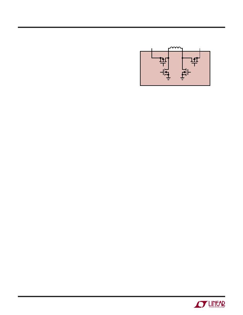
�BUCK-BOOST� CONVERTER� OPERATION�
�PWM� Mode� Operation�
�When� the� PWM� pin� is� held� high,� the� LTC3522� buck-boost�
�converter� operates� in� a� constant� frequency� PWM� mode� with�
�voltage� mode� control.� A� proprietary� switching� algorithm�
�allows� the� converter� to� switch� between� buck,� buck-boost�
�and� boost� modes� without� discontinuity� in� inductor� cur-�
�rent� or� loop� characteristics.� The� switch� topology� for� the�
�buck-boost� converter� is� shown� in� Figure� 1.�
�3522� F01�
�Figure� 1.� Buck-Boost� Switch� Topology�
�When� the� input� voltage� is� signi?cantly� greater� than� the�
�output� voltage,� the� buck-boost� converter� operates� in�
�buck� mode.� Switch� D� turns� on� continuously� and� switch�
�C� remains� off.� Switches� A� and� B� are� pulse� width� modu-�
�lated� to� produce� the� required� duty� cycle� to� support� the�
�output� regulation� voltage.� As� the� input� voltage� decreases,�
�switch� A� remains� on� for� a� larger� portion� of� the� switching�
�cycle.� When� the� duty� cycle� reaches� approximately� 85%,�
�the� switch� pair� AC� begins� turning� on� for� a� small� fraction�
�of� the� switching� period.� As� the� input� voltage� decreases�
�further,� the� AC� switch� pair� remains� on� for� longer� durations�
�and� the� duration� of� the� BD� phase� decreases� proportionally.�
�As� the� input� voltage� drops� below� the� output� voltage,� the�
�AC� phase� will� eventually� increase� to� the� point� that� there� is�
�no� longer� any� BD� phase.� At� this� point,� switch� A� remains� on�
�continuously� while� switch� pair� CD� is� pulse� width� modu-�
�lated� to� obtain� the� desired� output� voltage.� At� this� point,�
�the� converter� is� operating� solely� in� boost� mode.�
�This� switching� algorithm� provides� a� seamless� transition�
�between� operating� modes� and� eliminates� discontinuities�
�in� average� inductor� current,� inductor� current� ripple,� and�
�loop� transfer� function� throughout� all� three� operational�
�modes.� These� advantages� result� in� increased� ef?ciency�
�and� stability� in� comparison� to� the� traditional� 4-switch�
�buck-boost� converter.�
�Error� Ampli?er� and� Compensation�
�The� buck-boost� converter� utilizes� a� voltage� mode� error�
�ampli?er� with� an� internal� compensation� network� as� shown�
�in� Figure� 2.�
�Notice� that� resistor� R2� of� the� external� resistor� divider�
�network� plays� an� integral� role� in� determining� the� frequency�
�3522fa�
�10�
�相关PDF资料 |
PDF描述 |
|---|---|
| LTC3523EUD-2#TRPBF | IC REG BUCK BOOST SYNC ADJ 16QFN |
| LTC3525ESC6-3.3#TRPBF | IC REG BST SYNC 3.3V 0.4A SC70-6 |
| LTC3526BEDC#TRPBF | IC REG BOOST SYNC ADJ 0.5A 6DFN |
| LTC3527EUD-1#TRPBF | IC REG BOOST SYNC ADJ DL 16QFN |
| LTC3528EDDB#TRPBF | IC REG BOOST SYNC ADJ 1A 8DFN |
相关代理商/技术参数 |
参数描述 |
|---|---|
| LTC3523 | 制造商:LINER 制造商全称:Linear Technology 功能描述:Synchronous 600mA Step-Up and 400mA Step-Down DC/DC Converters |
| LTC3523EUD#PBF | 功能描述:IC REG BUCK BOOST SYNC ADJ 16QFN RoHS:是 类别:集成电路 (IC) >> PMIC - 稳压器 - DC DC 开关稳压器 系列:- 标准包装:250 系列:- 类型:降压(降压) 输出类型:固定 输出数:1 输出电压:1.2V 输入电压:2.05 V ~ 6 V PWM 型:电压模式 频率 - 开关:2MHz 电流 - 输出:500mA 同步整流器:是 工作温度:-40°C ~ 85°C 安装类型:表面贴装 封装/外壳:6-UFDFN 包装:带卷 (TR) 供应商设备封装:6-SON(1.45x1) 产品目录页面:1032 (CN2011-ZH PDF) 其它名称:296-25628-2 |
| LTC3523EUD#TRPBF | 功能描述:IC REG BUCK BOOST SYNC ADJ 16QFN RoHS:是 类别:集成电路 (IC) >> PMIC - 稳压器 - DC DC 开关稳压器 系列:- 标准包装:2,500 系列:- 类型:降压(降压) 输出类型:固定 输出数:1 输出电压:1.2V,1.5V,1.8V,2.5V 输入电压:2.7 V ~ 20 V PWM 型:- 频率 - 开关:- 电流 - 输出:50mA 同步整流器:是 工作温度:-40°C ~ 125°C 安装类型:表面贴装 封装/外壳:10-TFSOP,10-MSOP(0.118",3.00mm 宽)裸露焊盘 包装:带卷 (TR) 供应商设备封装:10-MSOP 裸露焊盘 |
| LTC3523EUD-2#PBF | 功能描述:IC REG BUCK BOOST SYNC ADJ 16QFN RoHS:是 类别:集成电路 (IC) >> PMIC - 稳压器 - DC DC 开关稳压器 系列:- 标准包装:2,500 系列:- 类型:降压(降压) 输出类型:固定 输出数:1 输出电压:1.2V,1.5V,1.8V,2.5V 输入电压:2.7 V ~ 20 V PWM 型:- 频率 - 开关:- 电流 - 输出:50mA 同步整流器:是 工作温度:-40°C ~ 125°C 安装类型:表面贴装 封装/外壳:10-TFSOP,10-MSOP(0.118",3.00mm 宽)裸露焊盘 包装:带卷 (TR) 供应商设备封装:10-MSOP 裸露焊盘 |
| LTC3523EUD-2#TRPBF | 功能描述:IC REG BUCK BOOST SYNC ADJ 16QFN RoHS:是 类别:集成电路 (IC) >> PMIC - 稳压器 - DC DC 开关稳压器 系列:- 标准包装:2,500 系列:- 类型:降压(降压) 输出类型:固定 输出数:1 输出电压:1.2V,1.5V,1.8V,2.5V 输入电压:2.7 V ~ 20 V PWM 型:- 频率 - 开关:- 电流 - 输出:50mA 同步整流器:是 工作温度:-40°C ~ 125°C 安装类型:表面贴装 封装/外壳:10-TFSOP,10-MSOP(0.118",3.00mm 宽)裸露焊盘 包装:带卷 (TR) 供应商设备封装:10-MSOP 裸露焊盘 |
发布紧急采购,3分钟左右您将得到回复。