- 您现在的位置:买卖IC网 > PDF目录1830 > LTC3534EGN#TRPBF (Linear Technology)IC REG BUCK BST SYNC 0.5A 16SSOP PDF资料下载
参数资料
| 型号: | LTC3534EGN#TRPBF |
| 厂商: | Linear Technology |
| 文件页数: | 11/20页 |
| 文件大小: | 0K |
| 描述: | IC REG BUCK BST SYNC 0.5A 16SSOP |
| 标准包装: | 2,500 |
| 类型: | 降压(降压),升压(升压) |
| 输出类型: | 可调式 |
| 输出数: | 1 |
| 输出电压: | 1.8 V ~ 7 V |
| 输入电压: | 2.4 V ~ 7 V |
| PWM 型: | Burst Mode? |
| 频率 - 开关: | 1MHz |
| 电流 - 输出: | 500mA |
| 同步整流器: | 是 |
| 工作温度: | -40°C ~ 85°C |
| 安装类型: | 表面贴装 |
| 封装/外壳: | 16-SSOP(0.154",3.90mm 宽) |
| 包装: | 带卷 (TR) |
| 供应商设备封装: | 16-SSOP |
�� �
�
�LTC3534�
�OPERATION�
�I� OUT(MAX)BURST� ?� BOOST� ≈�
�125� ?� V� IN�
�η� ?I� LOAD�
�25μA� +� I� LOAD�
�In Burst Mode operation the typical maximum average�
�output� currents� in� the� three� operating� regions,� buck,� four�
�switch,� and� boost� are� given� by:�
�I� OUT(MAX)BURST–BUCK� ≈� 100mA;�
�Burst� Mode� operation� –� buck� region:� V� IN� >� V� OUT�
�I� OUT(MAX)BURST–FOUR_SWITCH� ≈� 125mA;�
�Burst� Mode� operation� –� four� switch� region:� V� IN� ≈� V� OUT�
�mA;�
�V� OUT�
�Burst� Mode� operation� –� boost� region:� V� IN� <� V� OUT�
�The� efficiency� below� 1mA� becomes� dominated� primarily�
�by� the� quiescent� current.� The� Burst� Mode� operation� ef-�
�ficiency� is� given� by:�
�Efficiency� ?�
�where� h� is� typically� 90%� during� Burst� Mode� operation.�
�A� graph� of� Burst� Mode� operation� maximum� output� current�
�vs� V� IN� (for� V� OUT� =� 5V)� is� provided� in� the� Typical� Perfor-�
�mance� Characteristics� section.�
�Burst� Mode� Operation� to� Fixed� Frequency� Transient�
�Response�
�In� Burst� Mode� operation,� the� compensation� network� is�
�not� used� and� V� C� is� disconnected� from� the� error� amplifier.�
�V� IN�
�13�
�During� long� periods� of� Burst� Mode� operation,� leakage�
�currents� in� the� external� components� or� on� the� PC� board�
�could� cause� the� compensation� capacitor� to� charge� (or�
�discharge),� which� could� result� in� a� large� output� transient�
�when� returning� to� fixed� frequency� mode� operation,� even�
�at� the� same� load� current.� To� prevent� this,� the� LTC3534�
�incorporates� an� active� clamp� circuit� that� holds� the� voltage�
�on� V� C� at� an� optimal� voltage� during� Burst� Mode� operation.�
�This� minimizes� any� output� transient� when� returning� to�
�fixed� frequency� mode� operation.� For� optimum� transient�
�response,� Type� III� compensation� is� also� recommended�
�to� broad� band� the� control� loop� and� roll� off� past� the� two�
�pole� response� of� the� output� LC� filter.� (See� Closing� the�
�Feedback� Loop).�
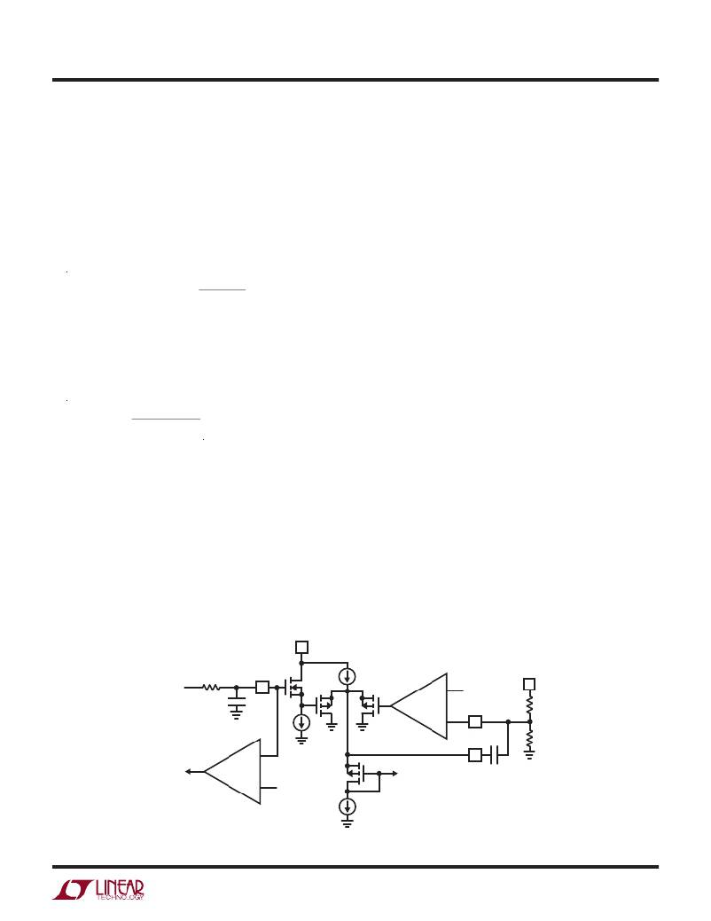
�Soft-Start�
�The� soft-start� function� is� combined� with� shutdown.� When�
�the� RUN/SS� pin� is� brought� above� 1V� typical,� the� LTC3534�
�is� enabled� but� the� error� amplifier� duty� cycle� is� clamped�
�from� V� C� .� A� detailed� diagram� of� this� function� is� shown� in�
�Figure� 3.� The� components� R� SS� and� C� SS� provide� a� slow�
�ramping� voltage� on� RUN/SS� to� provide� a� soft-start� func-�
�tion.� To� ensure� that� V� C� is� not� being� clamped,� RUN/SS�
�must� be� raised� to� 2.4V� or� above.� The� IC� must� be� enabled�
�(even� with� a� soft-start)� commanding� PWM� mode.� Once�
�the� LTC3534� is� in� regulation,� then� Burst� Mode� operation�
�can� be� commanded.�
�ENABLE�
�SIGNAL�
�R� SS�
�RUN/SS�
�2�
�C� SS�
�+�
�ERROR�
�AMP�
�–�
�1V�
�FB�
�15�
�V� OUT�
�11�
�R1�
�CHIP�
�ENABLE�
�+�
�–�
�1V�
�V� CI�
�TO� PWM�
�COMPARATORS�
�V� C�
�14�
�C� P1�
�R2�
�3534� F03�
�Figure� 3.� Soft-Start� Circuitry�
�3534fb�
�For� more� information� www.linear.com/LTC3534�
�11�
�相关PDF资料 |
PDF描述 |
|---|---|
| LTC3535EDD#PBF | IC REG BST SYNC ADJ 0.55A 12DFN |
| LTC3536IMSE#TRPBF | IC REG BUCK BST SYNC ADJ 12MSOP |
| LTC3538EDCB#TRPBF | IC REG BUCK BOOST SYNC ADJ 8DFN |
| LTC3539EDCB-2#TRPBF | IC REG BOOST SYNC ADJ 2A 8DFN |
| LTC3542IDC#TRMPBF | IC REG BUCK SYNC ADJ 0.5A 6DFN |
相关代理商/技术参数 |
参数描述 |
|---|---|
| LTC3535 | 制造商:LINER 制造商全称:Linear Technology 功能描述:Dual Channel 550mA 1MHz Synchronous Step-Up DC/DC Converter |
| LTC3535EDD#PBF | 功能描述:IC REG BST SYNC ADJ 0.55A 12DFN RoHS:是 类别:集成电路 (IC) >> PMIC - 稳压器 - DC DC 开关稳压器 系列:- 设计资源:Design Support Tool 标准包装:1 系列:- 类型:升压(升压) 输出类型:固定 输出数:1 输出电压:3V 输入电压:0.75 V ~ 2 V PWM 型:- 频率 - 开关:- 电流 - 输出:100mA 同步整流器:是 工作温度:-40°C ~ 85°C 安装类型:表面贴装 封装/外壳:SOT-23-5 细型,TSOT-23-5 包装:剪切带 (CT) 供应商设备封装:TSOT-23-5 其它名称:AS1323-BTTT-30CT |
| LTC3535EDD#PBF | 制造商:Linear Technology 功能描述:DC/DC CONVERTER IC |
| LTC3535EDD#TRPBF | 功能描述:IC REG BST SYNC ADJ 0.55A 12DFN RoHS:是 类别:集成电路 (IC) >> PMIC - 稳压器 - DC DC 开关稳压器 系列:- 标准包装:2,500 系列:- 类型:降压(降压) 输出类型:固定 输出数:1 输出电压:1.2V,1.5V,1.8V,2.5V 输入电压:2.7 V ~ 20 V PWM 型:- 频率 - 开关:- 电流 - 输出:50mA 同步整流器:是 工作温度:-40°C ~ 125°C 安装类型:表面贴装 封装/外壳:10-TFSOP,10-MSOP(0.118",3.00mm 宽)裸露焊盘 包装:带卷 (TR) 供应商设备封装:10-MSOP 裸露焊盘 |
| LTC3535EDD-PBF | 制造商:LINER 制造商全称:Linear Technology 功能描述:Dual Channel 550mA 1MHz Synchronous Step-Up DC/DC Converter |
发布紧急采购,3分钟左右您将得到回复。