- 您现在的位置:买卖IC网 > PDF目录44993 > LTC3810IG#TR (LINEAR TECHNOLOGY CORP) SWITCHING CONTROLLER, PDSO28 PDF资料下载
参数资料
| 型号: | LTC3810IG#TR |
| 厂商: | LINEAR TECHNOLOGY CORP |
| 元件分类: | 稳压器 |
| 英文描述: | SWITCHING CONTROLLER, PDSO28 |
| 封装: | 5.30 MM, PLASTIC, SSOP-28 |
| 文件页数: | 5/36页 |
| 文件大小: | 495K |
| 代理商: | LTC3810IG#TR |
第1页第2页第3页第4页当前第5页第6页第7页第8页第9页第10页第11页第12页第13页第14页第15页第16页第17页第18页第19页第20页第21页第22页第23页第24页第25页第26页第27页第28页第29页第30页第31页第32页第33页第34页第35页第36页
LTC3810
13
3810fb
Fault Monitoring/Protection
Constant on-time current mode architecture provides ac-
curate cycle-by-cycle current limit protection—a feature
that is very important for protecting the high voltage power
supply from output short circuits. The cycle-by-cycle cur-
rent monitor guarantees that the inductor current will never
exceed the value programmed on the VRNG pin.
Foldback current limiting provides further protection if the
output is shorted to ground. As VFB drops, the buffered
current threshold voltage ITHB is pulled down and clamped
to 1V. This reduces the inductor valley current level to
one-sixth of its maximum value as VFB approaches 0V.
Foldback current limiting is disabled at start-up.
Overvoltage and undervoltage comparators OV and UV
pull the PGOOD output low if the output feedback voltage
exits a ±10% window around the regulation point after the
internal 120μs power bad mask timer expires. Furthermore,
in an overvoltage condition, M1 is turned off and M2 is
turned on immediately and held on until the overvoltage
condition clears.
The LTC3810 provides two undervoltage lockout com-
parators—one for the INTVCC/DRVCC supply and one for
the input supply VIN. The INTVCC UV threshold is 6.2V to
guarantee that the MOSFETs have sufcient gate drive volt-
age before turning on. The VIN UV threshold (UVIN pin) is
0.8V with 10% hysteresis which allows programming the
VIN threshold with the appropriate resistor divider con-
nected to VIN. If either comparator inputs are under the
UV threshold, the LTC3810 is shut down and the drivers
are turned off.
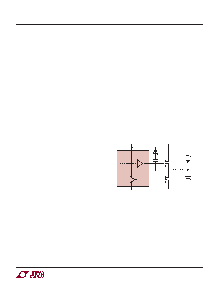
Strong Gate Drivers
The LTC3810 contains very low impedance drivers capable
of supplying amps of current to slew large MOSFET gates
quickly. This minimizes transition losses and allows paral-
leling MOSFETs for higher current applications. A 100V
oating high side driver drives the top side MOSFET and
a low side driver drives the bottom side MOSFET (see
Figure 3). The bottom side driver is supplied directly
from the DRVCC pin. The top MOSFET drivers are biased
from oating bootstrap capacitor, CB, which normally is
recharged during each off cycle through an external diode
from DRVCC when the top MOSFET turns off. In pulse
skip mode operation, where it is possible that the bottom
MOSFET will be off for an extended period of time, an
internal timeout guarantees that the bottom MOSFET is
turned on at least once every 25μs for one on-time period
to refresh the bootstrap capacitor.
The bottom driver has an additional feature that helps
minimize the possibility of external MOSFET shoot-through.
When the top MOSFET turns on, the switch node dV/dt
pulls up the bottom MOSFET’s internal gate through the
Miller capacitance, even when the bottom driver is holding
the gate terminal at ground. If the gate is pulled up high
enough, shoot-through between the top side and bottom
side MOSFETs can occur. To prevent this from occurring,
the bottom driver return is brought out as a separate pin
(BGRTN) so that a negative supply can be used to reduce
the effect of the Miller pull-up. For example, if a –2V sup-
ply is used on BGRTN, the switch node dV/dt could pull
the gate up 2V before the VGS of the bottom MOSFET has
more than 0V across it.
IC/Driver Supply Power
The LTC3810’s internal control circuitry and top and bottom
MOSFET drivers operate from a supply voltage (INTVCC,
DRVCC pins) in the range of 6.2V to 14V. The LTC3810
has two integrated linear regulator controllers to easily
generate this IC/driver supply from either the high voltage
input or from the output voltage. For best efciency the
supply is derived from the input voltage during start-up
and then derived from the lower voltage output as soon
as the output is higher than 6.7V. Alternatively, the supply
can be derived from the input continuously if the output
Figure 3. Floating TG Driver Supply and Negative BG Return
OPERATION
BOOST
TG
SW
BG
BGRTN
DRVCC
LTC3810
M1
M2
+
VIN
CIN
VOUT
COUT
DB
CB
L
3810 F03
0V TO –5V
相关PDF资料 |
PDF描述 |
|---|---|
| LTC3810EG | SWITCHING CONTROLLER, PDSO28 |
| LTC3812EFE-5 | 1 A SWITCHING CONTROLLER, PDSO16 |
| LTC3812IFE-5#TR | 1 A SWITCHING CONTROLLER, PDSO16 |
| LTC3812EFE-5#TR | 1 A SWITCHING CONTROLLER, PDSO16 |
| LTC3812IFE-5 | 1 A SWITCHING CONTROLLER, PDSO16 |
相关代理商/技术参数 |
参数描述 |
|---|---|
| LTC3810IUH-5#PBF | 功能描述:IC REG CTRLR BUCK PWM CM 32-QFN RoHS:是 类别:集成电路 (IC) >> PMIC - 稳压器 - DC DC 切换控制器 系列:- 标准包装:2,500 系列:- PWM 型:电流模式 输出数:1 频率 - 最大:500kHz 占空比:96% 电源电压:4 V ~ 36 V 降压:无 升压:是 回扫:无 反相:无 倍增器:无 除法器:无 Cuk:无 隔离:无 工作温度:-40°C ~ 125°C 封装/外壳:24-WQFN 裸露焊盘 包装:带卷 (TR) |
| LTC3810IUH-5#TRPBF | 功能描述:IC REG CTRLR BUCK PWM CM 32-QFN RoHS:是 类别:集成电路 (IC) >> PMIC - 稳压器 - DC DC 切换控制器 系列:- 标准包装:2,500 系列:- PWM 型:电流模式 输出数:1 频率 - 最大:500kHz 占空比:96% 电源电压:4 V ~ 36 V 降压:无 升压:是 回扫:无 反相:无 倍增器:无 除法器:无 Cuk:无 隔离:无 工作温度:-40°C ~ 125°C 封装/外壳:24-WQFN 裸露焊盘 包装:带卷 (TR) |
| LTC3811EG#PBF | 功能描述:IC REG CTRLR BUCK PWM CM 36-SSOP RoHS:是 类别:集成电路 (IC) >> PMIC - 稳压器 - DC DC 切换控制器 系列:PolyPhase® 标准包装:2,500 系列:- PWM 型:电流模式 输出数:1 频率 - 最大:500kHz 占空比:96% 电源电压:4 V ~ 36 V 降压:无 升压:是 回扫:无 反相:无 倍增器:无 除法器:无 Cuk:无 隔离:无 工作温度:-40°C ~ 125°C 封装/外壳:24-WQFN 裸露焊盘 包装:带卷 (TR) |
| LTC3811EG#TRPBF | 功能描述:IC REG CTRLR BUCK PWM CM 36-SSOP RoHS:是 类别:集成电路 (IC) >> PMIC - 稳压器 - DC DC 切换控制器 系列:PolyPhase® 标准包装:2,500 系列:- PWM 型:电流模式 输出数:1 频率 - 最大:500kHz 占空比:96% 电源电压:4 V ~ 36 V 降压:无 升压:是 回扫:无 反相:无 倍增器:无 除法器:无 Cuk:无 隔离:无 工作温度:-40°C ~ 125°C 封装/外壳:24-WQFN 裸露焊盘 包装:带卷 (TR) |
| LTC3811EUHF#PBF | 功能描述:IC REG CTRLR BUCK PWM CM 38-QFN RoHS:是 类别:集成电路 (IC) >> PMIC - 稳压器 - DC DC 切换控制器 系列:PolyPhase® 标准包装:2,500 系列:- PWM 型:电流模式 输出数:1 频率 - 最大:500kHz 占空比:96% 电源电压:4 V ~ 36 V 降压:无 升压:是 回扫:无 反相:无 倍增器:无 除法器:无 Cuk:无 隔离:无 工作温度:-40°C ~ 125°C 封装/外壳:24-WQFN 裸露焊盘 包装:带卷 (TR) |
发布紧急采购,3分钟左右您将得到回复。