- 您现在的位置:买卖IC网 > PDF目录69007 > LTC3823EUH (LINEAR TECHNOLOGY CORP) 4 A SWITCHING CONTROLLER, 200 kHz SWITCHING FREQ-MAX, PQCC32 PDF资料下载
参数资料
| 型号: | LTC3823EUH |
| 厂商: | LINEAR TECHNOLOGY CORP |
| 元件分类: | 稳压器 |
| 英文描述: | 4 A SWITCHING CONTROLLER, 200 kHz SWITCHING FREQ-MAX, PQCC32 |
| 封装: | 5 X 5 MM, PLASTIC, MO-220WHHD, QFN-32 |
| 文件页数: | 11/24页 |
| 文件大小: | 345K |
| 代理商: | LTC3823EUH |
LTC3823
3823fb
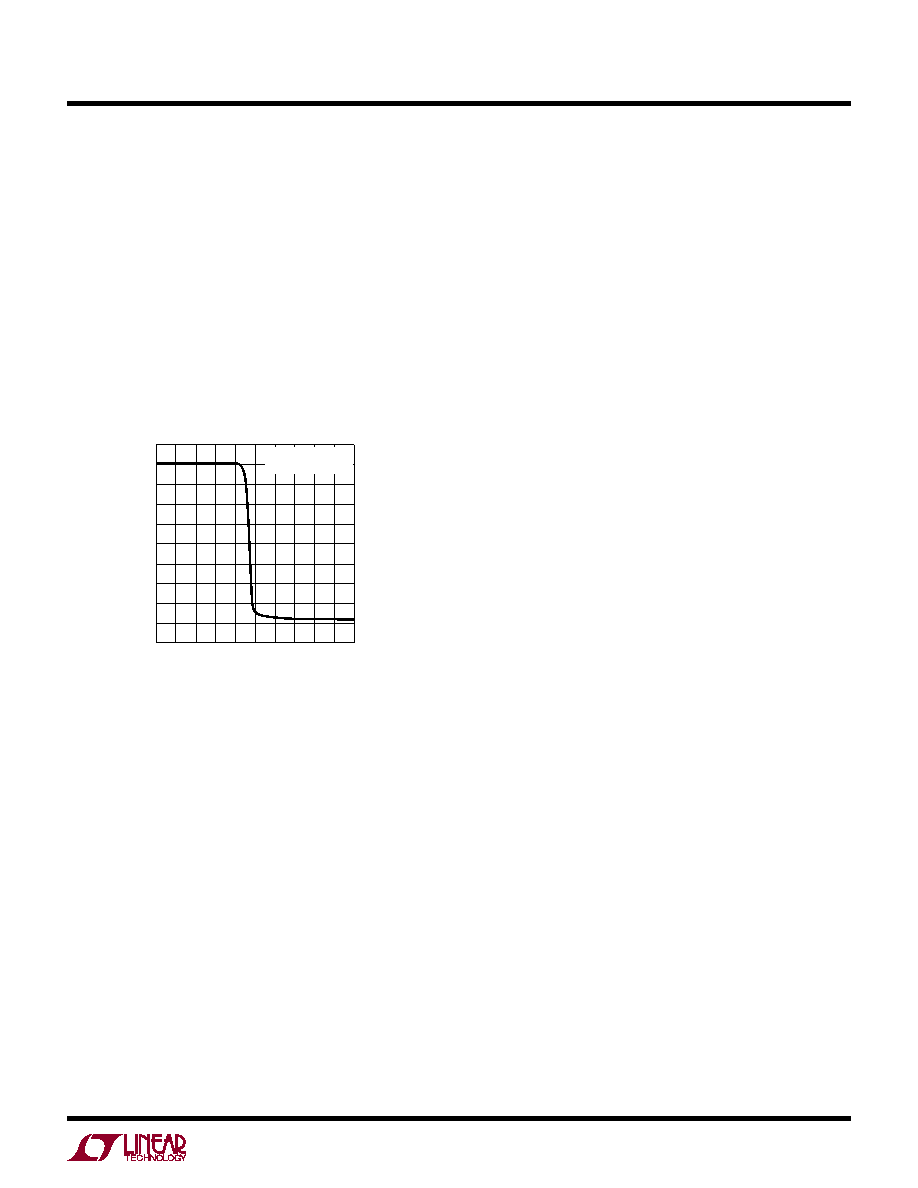
on the Z0 pin, the TG low BG high dead time can be pro-
grammed. Because the dead time is a strong function of
the load current and the type of MOSFET used, users need
to be careful to optimize the dead time for their particular
applications. Figure 11 shows the relation between the TG
Low BG high dead time by varying the Z0 voltages. For
an application using LTC3823 with load current of 5A and
IR7811W MOSFETs, the dead time could be optimized. To
make sure that there is no shoot-through under all condi-
tions, a dead time of 70ns is selected. This corresponds to
a DC voltage about 2.4V on Z0 pin. This voltage can easily
be generated with a resistor divider off INTVCC.
applications information
DC I2R loss. For example, if RDS(ON) = 0.01Ω and RL =
0.005
Ω, the loss will range from 15mW to 1.5W as the
output current varies from 1A to 10A.
2. Transition loss. This loss arises from the brief amount
of time the top MOSFET spends in the saturated region
during switch node transitions. It depends upon the
input voltage, load current, driver strength and MOSFET
capacitance, among other factors. The loss is significant
at input voltages above 20V and can be estimated from:
Transition Loss
(1.7A–1) VIN2 IOUT CRSS f
3. INTVCC current. This is the sum of the MOSFET driver
and control currents.
4. CIN loss. The input capacitor has the difficult job of
filtering the large RMS input current to the regulator. It
must have a very low ESR to minimize the AC I2R loss and
sufficient capacitance to prevent the RMS current from
causing additional upstream losses in fuses or batteries.
Other losses, including COUT ESR loss, Schottky diode D1
conduction loss during dead time and inductor core loss
generally account for less than 2% additional loss.
Whenmakingadjustmentstoimproveefficiency,the input
current is the best indicator of changes in efficiency. If you
make a change and the input current decreases, then the
efficiency has increased. If there is no change in input
current, then there is no change in efficiency.
Checking Transient Response
The regulator loop response can be checked by looking
at the load transient response. Switching regulators take
several cycles to respond to a step in load current. When
a load step occurs, VOUT immediately shifts by an amount
equal to
ΔILOAD (ESR), where ESR is the effective series
resistance of COUT. ΔILOAD also begins to charge or dis-
chargeCOUTgeneratingafeedbackerrorsignalusedbythe
regulator to return VOUT to its steady-state value. During
this recovery time, VOUT can be monitored for overshoot
or ringing that would indicate a stability problem. The ITh
pin external components shown in Figure 12 will provide
adequate compensation for most applications. For a
detailed explanation of switching control loop theory see
Application Note 76.
Z0 VOLTAGE (V)
0
TG
LOW
TO
BG
HIGH
DEADTIME
(ns)
120
160
200
4
3823 F11
80
40
100
140
180
60
20
0
1
0.5
2
1.5
3 3.5
4.5
2.5
5
IOUT = 2A
FIGURE 12 CIRCUIT
Figure 11. TG Low BG High Dead Time vs Z0 Voltage
Efficiency Considerations
The percent efficiency of a switching regulator is equal to
the output power divided by the input power times 100%.
It is often useful to analyze individual losses to determine
what is limiting the efficiency and which change would
produce the most improvement. Although all dissipative
elements in the circuit produce losses, four main sources
account for most of the losses in LTC3823 circuits:
1. DC I2R losses. These arise from the resistances of the
MOSFETs, inductor and PC board traces and cause the
efficiency to drop at high output currents. In continuous
mode the average output current flows through L, but is
chopped between the top and bottom MOSFETs. If the two
MOSFETs have approximately the same RDS(ON), then the
resistance of one MOSFET can simply be summed with
the resistances of L and the board traces to obtain the
相关PDF资料 |
PDF描述 |
|---|---|
| LTC3823EGN | 4 A SWITCHING CONTROLLER, 200 kHz SWITCHING FREQ-MAX, PDSO28 |
| LTC3823EUH#TR | 4 A SWITCHING CONTROLLER, 200 kHz SWITCHING FREQ-MAX, PQCC32 |
| LTC3823EGN#TR | 4 A SWITCHING CONTROLLER, 200 kHz SWITCHING FREQ-MAX, PDSO28 |
| LTC3827IUH | 3 A DUAL SWITCHING CONTROLLER, 580 kHz SWITCHING FREQ-MAX, PQCC32 |
| LTC3827IUH#TR | 3 A DUAL SWITCHING CONTROLLER, 580 kHz SWITCHING FREQ-MAX, PQCC32 |
相关代理商/技术参数 |
参数描述 |
|---|---|
| LTC3823EUH#PBF | 功能描述:IC REG CTRLR BUCK PWM CM 32-QFN RoHS:是 类别:集成电路 (IC) >> PMIC - 稳压器 - DC DC 切换控制器 系列:- 标准包装:2,000 系列:- PWM 型:电流模式 输出数:1 频率 - 最大:1MHz 占空比:50% 电源电压:9 V ~ 10 V 降压:无 升压:是 回扫:是 反相:无 倍增器:无 除法器:无 Cuk:无 隔离:无 工作温度:-40°C ~ 85°C 封装/外壳:8-TSSOP(0.173",4.40mm 宽) 包装:带卷 (TR) |
| LTC3823EUH#TRPBF | 功能描述:IC REG CTRLR BUCK PWM CM 32-QFN RoHS:是 类别:集成电路 (IC) >> PMIC - 稳压器 - DC DC 切换控制器 系列:- 标准包装:2,500 系列:- PWM 型:电流模式 输出数:1 频率 - 最大:500kHz 占空比:96% 电源电压:4 V ~ 36 V 降压:无 升压:是 回扫:无 反相:无 倍增器:无 除法器:无 Cuk:无 隔离:无 工作温度:-40°C ~ 125°C 封装/外壳:24-WQFN 裸露焊盘 包装:带卷 (TR) |
| LTC3823IGN#PBF | 功能描述:IC REG CTRLR BUCK PWM CM 28-SSOP RoHS:是 类别:集成电路 (IC) >> PMIC - 稳压器 - DC DC 切换控制器 系列:- 标准包装:2,000 系列:- PWM 型:电流模式 输出数:1 频率 - 最大:1MHz 占空比:50% 电源电压:9 V ~ 10 V 降压:无 升压:是 回扫:是 反相:无 倍增器:无 除法器:无 Cuk:无 隔离:无 工作温度:-40°C ~ 85°C 封装/外壳:8-TSSOP(0.173",4.40mm 宽) 包装:带卷 (TR) |
| LTC3823IGN#PBF | 制造商:Linear Technology 功能描述:IC SYNC STEP-DOWN DC/DC CTRL SSOP-28 |
| LTC3823IGN#TRPBF | 功能描述:IC REG CTRLR BUCK PWM CM 28-SSOP RoHS:是 类别:集成电路 (IC) >> PMIC - 稳压器 - DC DC 切换控制器 系列:- 标准包装:2,500 系列:- PWM 型:电流模式 输出数:1 频率 - 最大:500kHz 占空比:96% 电源电压:4 V ~ 36 V 降压:无 升压:是 回扫:无 反相:无 倍增器:无 除法器:无 Cuk:无 隔离:无 工作温度:-40°C ~ 125°C 封装/外壳:24-WQFN 裸露焊盘 包装:带卷 (TR) |
发布紧急采购,3分钟左右您将得到回复。