- 您现在的位置:买卖IC网 > PDF目录69007 > LTC3827IUH#TR (LINEAR TECHNOLOGY CORP) 3 A DUAL SWITCHING CONTROLLER, 580 kHz SWITCHING FREQ-MAX, PQCC32 PDF资料下载
参数资料
| 型号: | LTC3827IUH#TR |
| 厂商: | LINEAR TECHNOLOGY CORP |
| 元件分类: | 稳压器 |
| 英文描述: | 3 A DUAL SWITCHING CONTROLLER, 580 kHz SWITCHING FREQ-MAX, PQCC32 |
| 封装: | 5 X 5 MM, PLASTIC, MO-220WHHD, QFN-32 |
| 文件页数: | 14/36页 |
| 文件大小: | 451K |
| 代理商: | LTC3827IUH#TR |
第1页第2页第3页第4页第5页第6页第7页第8页第9页第10页第11页第12页第13页当前第14页第15页第16页第17页第18页第19页第20页第21页第22页第23页第24页第25页第26页第27页第28页第29页第30页第31页第32页第33页第34页第35页第36页

LTC3827
21
3827ff
APPLICATIONS INFORMATION
gate charge current, may be supplied by either the 5.25V
VIN LDO or the 7.5V EXTVCC LDO. When the voltage on
the EXTVCC pin is less than 4.7V, the VIN LDO is enabled.
Power dissipation for the IC in this case is highest and is
equal to VIN INTVCC. The gate charge current is dependent
on operating frequency as discussed in the Efciency
Considerations section. The junction temperature can be
estimated by using the equations given in Note 2 of the
Electrical Characteristics. For example, the LTC3827 INTVCC
current is limited to less than 24mA from a 24V supply
when in the G package and not using the EXTVCC supply:
TJ = 70°C + (24mA)(24V)(95°C/W) = 125°C
To prevent the maximum junction temperature from being
exceeded, the input supply current must be checked while
operating in continuous conduction mode (PLLIN/MODE
= INTVCC) at maximum VIN.
When the voltage applied to EXTVCC rises above 4.7V, the
VIN LDO is turned off and the EXTVCC LDO is enabled. The
EXTVCC LDO remains on as long as the voltage applied to
EXTVCC remains above 4.5V. The EXTVCC LDO attempts
to regulate the INTVCC voltage to 7.5V, so while EXTVCC
is less than 7.5V, the LDO is in dropout and the INTVCC
voltage is approximately equal to EXTVCC. When EXTVCC
is greater than 7.5V up to an absolute maximum of 10V,
INTVCC is regulated to 7.5V.
Using the EXTVCC LDO allows the MOSFET driver and
control power to be derived from one of the LTC3827’s
switching regulator outputs (4.7V ≤ VOUT ≤ 10V) during
normal operation and from the VIN LDO when the output
is out of regulation (e.g., start-up, short-circuit). If more
current is required through the EXTVCC LDO than is spec-
ied, an external Schottky diode can be added between the
EXTVCC and INTVCC pins. Do not apply more than 10V to
the EXTVCC pin and make sure than EXTVCC ≤ VIN.
Signicant efciency and thermal gains can be realized
by powering INTVCC from the output, since the VIN cur-
rent resulting from the driver and control currents will be
scaled by a factor of (Duty Cycle)/(Switcher Efciency). For
5V to 10V regulator outputs, this means connecting the
EXTVCC pin directly to VOUT. Tying the EXTVCC pin to a 5V
supply reduces the junction temperature in the previous
example from 125°C to:
TJ = 70°C + (24mA)(5V)(95°C/W) = 81°C
However, for 3.3V and other low voltage outputs, addi-
tional circuitry is required to derive INTVCC power from
the output.
The following list summarizes the four possible connec-
tions for EXTVCC:
1. EXTVCC Left Open (or Grounded). This will cause
INTVCC to be powered from the internal 5.25V regulator
resulting in an efciency penalty of up to 10% at high
input voltages.
2. EXTVCC Connected directly to VOUT. This is the normal
connection for a 5V to 10V regulator and provides the
highest efciency.
3. EXTVCC Connected to an External supply. If an external
supply is available in the 5V to 10V range, it may be
used to power EXTVCC providing it is compatible with
the MOSFET gate drive requirements.
4. EXTVCCConnectedtoanOutput-DerivedBoostNetwork.
For 3.3V and other low voltage regulators, efciency
gains can still be realized by connecting EXTVCC to an
output-derived voltage that has been boosted to greater
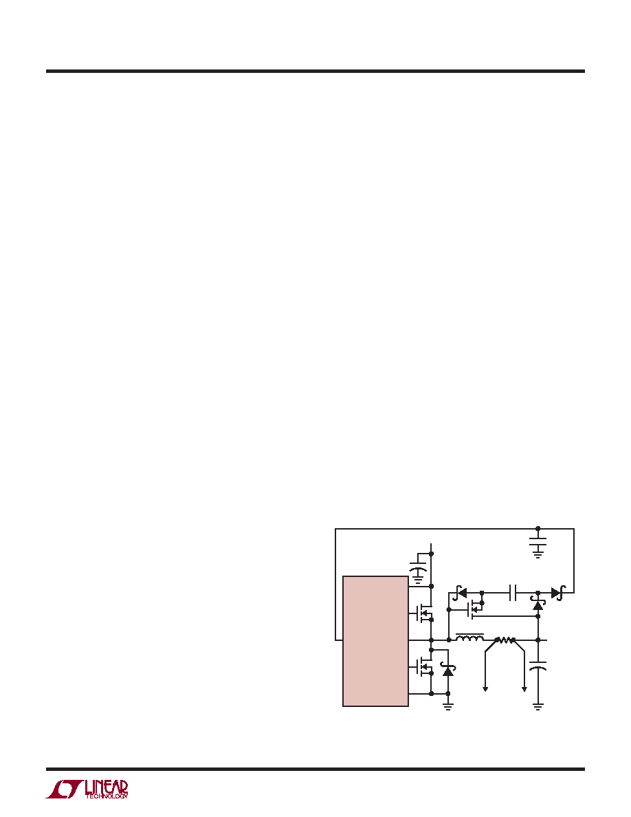
than 4.7V. This can be done with the capacitive charge
pump shown in Figure 8.
Figure 8. Capacitive Charge Pump for EXTVCC
EXTVCC
VIN
TG1
SW
BG1
PGND
LTC3827
RSENSE
VOUT
VN2222LL
+
COUT
3827 F08
N-CH
+
CIN
1μF
VIN
L1
BAT85
0.22μF
相关PDF资料 |
PDF描述 |
|---|---|
| LTC4010EFE | 0.2 A BATTERY CHARGE CONTROLLER, 640 kHz SWITCHING FREQ-MAX, PDSO16 |
| LTC4065LXEDC#PBF | 1-CHANNEL POWER SUPPLY SUPPORT CKT, PDSO6 |
| LTC4065LXEDC#TRM | 1-CHANNEL POWER SUPPLY SUPPORT CKT, PDSO6 |
| LTC4065LEDC#PBF | 1-CHANNEL POWER SUPPLY SUPPORT CKT, PDSO6 |
| LTC4065LXEDC#TRMPBF | 1-CHANNEL POWER SUPPLY SUPPORT CKT, PDSO6 |
相关代理商/技术参数 |
参数描述 |
|---|---|
| LTC3828EG#PBF | 功能描述:IC REG CTRLR BUCK PWM CM 28-SSOP RoHS:是 类别:集成电路 (IC) >> PMIC - 稳压器 - DC DC 切换控制器 系列:PolyPhase® 标准包装:2,000 系列:- PWM 型:电流模式 输出数:1 频率 - 最大:1MHz 占空比:50% 电源电压:9 V ~ 10 V 降压:无 升压:是 回扫:是 反相:无 倍增器:无 除法器:无 Cuk:无 隔离:无 工作温度:-40°C ~ 85°C 封装/外壳:8-TSSOP(0.173",4.40mm 宽) 包装:带卷 (TR) |
| LTC3828EG#TRPBF | 功能描述:IC REG CTRLR BUCK PWM CM 28-SSOP RoHS:是 类别:集成电路 (IC) >> PMIC - 稳压器 - DC DC 切换控制器 系列:PolyPhase® 标准包装:4,500 系列:PowerWise® PWM 型:控制器 输出数:1 频率 - 最大:1MHz 占空比:95% 电源电压:2.8 V ~ 5.5 V 降压:是 升压:无 回扫:无 反相:无 倍增器:无 除法器:无 Cuk:无 隔离:无 工作温度:-40°C ~ 125°C 封装/外壳:6-WDFN 裸露焊盘 包装:带卷 (TR) 配用:LM1771EVAL-ND - BOARD EVALUATION LM1771 其它名称:LM1771SSDX |
| LTC3828EUH | 制造商:Linear Technology 功能描述:DC DC Cntrlr Dual-OUT Sync Step Down 4.5V to 28V Input 32-Pin QFN EP |
| LTC3828EUH#PBF | 功能描述:IC REG CTRLR BUCK PWM CM 32-QFN RoHS:是 类别:集成电路 (IC) >> PMIC - 稳压器 - DC DC 切换控制器 系列:PolyPhase® 标准包装:4,500 系列:PowerWise® PWM 型:控制器 输出数:1 频率 - 最大:1MHz 占空比:95% 电源电压:2.8 V ~ 5.5 V 降压:是 升压:无 回扫:无 反相:无 倍增器:无 除法器:无 Cuk:无 隔离:无 工作温度:-40°C ~ 125°C 封装/外壳:6-WDFN 裸露焊盘 包装:带卷 (TR) 配用:LM1771EVAL-ND - BOARD EVALUATION LM1771 其它名称:LM1771SSDX |
| LTC3828EUH#TRPBF | 功能描述:IC REG CTRLR BUCK PWM CM 32-QFN RoHS:是 类别:集成电路 (IC) >> PMIC - 稳压器 - DC DC 切换控制器 系列:PolyPhase® 标准包装:4,500 系列:PowerWise® PWM 型:控制器 输出数:1 频率 - 最大:1MHz 占空比:95% 电源电压:2.8 V ~ 5.5 V 降压:是 升压:无 回扫:无 反相:无 倍增器:无 除法器:无 Cuk:无 隔离:无 工作温度:-40°C ~ 125°C 封装/外壳:6-WDFN 裸露焊盘 包装:带卷 (TR) 配用:LM1771EVAL-ND - BOARD EVALUATION LM1771 其它名称:LM1771SSDX |
发布紧急采购,3分钟左右您将得到回复。