- 您现在的位置:买卖IC网 > PDF目录15310 > LTC3830-1ES8#TRPBF (Linear Technology)IC REG CTRLR BUCK PWM VM 8-SOIC PDF资料下载
参数资料
| 型号: | LTC3830-1ES8#TRPBF |
| 厂商: | Linear Technology |
| 文件页数: | 12/24页 |
| 文件大小: | 0K |
| 描述: | IC REG CTRLR BUCK PWM VM 8-SOIC |
| 标准包装: | 2,500 |
| PWM 型: | 电压模式 |
| 输出数: | 1 |
| 频率 - 最大: | 250kHz |
| 占空比: | 95% |
| 电源电压: | 3 V ~ 8 V |
| 降压: | 是 |
| 升压: | 无 |
| 回扫: | 无 |
| 反相: | 无 |
| 倍增器: | 无 |
| 除法器: | 无 |
| Cuk: | 无 |
| 隔离: | 无 |
| 工作温度: | -40°C ~ 85°C |
| 封装/外壳: | 8-SOIC(0.154",3.90mm 宽) |
| 包装: | 带卷 (TR) |
�� �
�
�LTC3830/LTC3830-1�
�APPLICATIO� S� I� FOR� ATIO�
�Input� Supply� Considerations/Charge� Pump�
�The� 16-lead� LTC3830� requires� four� supply� voltages� to�
�operate:� V� IN� for� the� main� power� input,� PV� CC1� and� PV� CC2� for�
�MOSFET� gate� drive� and� a� clean,� low� ripple� V� CC� for� the�
�LTC3830� internal� circuitry� (Figure� 6).� The� LTC3830-1� and�
�the� 8-lead� LTC3830� have� the� PV� CC2� and� V� CC� pins� tied�
�together� inside� the� package� (Figure� 7).� This� pin,� brought�
�out� as� V� CC� /PV� CC2� ,� has� the� same� low� ripple� requirements�
�as� the� 16-lead� part,� but� must� also� be� able� to� supply� the� gate�
�drive� current� to� Q2.�
�In� many� applications,� V� CC� can� be� powered� from� V� IN�
�throughanRCfilter.Thissupplycanbeaslowas3V.The�
�low� quiescent� current� (typically� 800� μ� A)� allows� the� use� of�
�relatively� large� filter� resistors� and� correspondingly� small�
�filter� capacitors.� 100� ?� and� 4.7� μ� F� usually� provide� ad-�
�equate� filtering� for� V� CC� .� For� best� performance,� connect� the�
�4.7� μ� F� bypass� capacitor� as� close� to� the� LTC3830� V� CC� pin� as�
�possible.�
�Gate� drive� for� the� top� N-channel� MOSFET� Q1� is� supplied�
�from� PV� CC1� .� This� supply� must� be� above� V� IN� (the� main�
�power� supply� input)� by� at� least� one� power� MOSFET� V� GS(ON)�
�for� efficient� operation.� An� internal� level� shifter� allows� PV� CC1�
�to� operate� at� voltages� above� V� CC� and� V� IN� ,� up� to� 14V� maxi-�
�mum.� This� higher� voltage� can� be� supplied� with� a� separate�
�supply,� or� it� can� be� generated� using� a� charge� pump.�
�Gate� drive� for� the� bottom� MOSFET� Q2� is� provided� through�
�PV� CC2� for� the� 16-lead� LTC3830� or� V� CC� /PV� CC2� for� the�
�LTC3830-1� and� the� 8-lead� LTC3830.� This� supply� only�
�needs� to� be� above� the� power� MOSFET� V� GS(ON)� for� efficient�
�operation.� PV� CC2� can� also� be� driven� from� the� same� supply/�
�charge� pump� for� the� PV� CC1� ,� or� it� can� be� connected� to� a�
�lower� supply� to� improve� efficiency.�
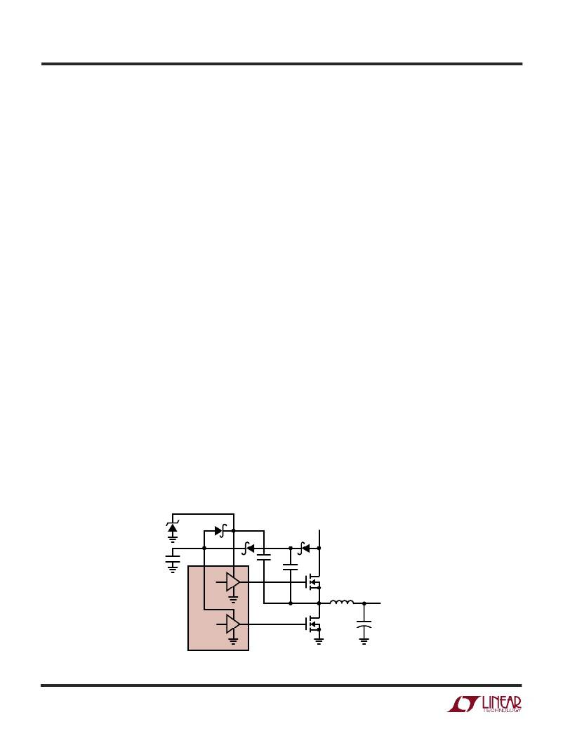
�Figure� 8� shows� a� tripling� charge� pump� circuit� that� can� be�
�used� to� provide� 2V� IN� and� 3V� IN� gate� drive� for� the� external�
�top� and� bottom� MOSFETs� respectively.� These� should� fully�
�enhance� MOSFETs� with� 5V� logic� level� thresholds.� This�
�circuit� provides� 3V� IN� –� 3V� F� to� PV� CC1� while� Q1� is� ON� and�
�2V� IN� –� 2V� F� to� PV� CC2� where� V� F� is� the� forward� voltage� of� the�
�Schottky� diodes.� The� circuit� requires� the� use� of� Schottky�
�diodes� to� minimize� forward� drop� across� the� diodes� at�
�start-up.� The� tripling� charge� pump� circuit� can� rectify� any�
�ringing� at� the� drain� of� Q2� and� provide� more� than� 3V� IN� at�
�PV� CC1� ;� a� 12V� zener� diode� should� be� included� from� PV� CC1�
�to� PGND� to� prevent� transients� from� damaging� the� circuitry�
�at� PV� CC1� or� the� gate� of� Q1.�
�The� charge� pump� capacitors� refresh� when� the� G2� pin� goes�
�high� and� the� switch� node� is� pulled� low� by� Q2.� The� G2� on-�
�time� becomes� narrow� when� LTC3830� operates� at� maxi-�
�mum� duty� cycle� (95%� typical),� which� can� occur� if� the� input�
�supply� rises� more� slowly� than� the� soft-start� capacitor� or�
�the� input� voltage� droops� during� load� transients.� If� the� G2�
�on-time� gets� so� narrow� that� the� switch� node� fails� to� pull�
�completely� to� ground,� the� charge� pump� voltage� may�
�collapse� or� fail� to� start,� causing� excessive� dissipation� in�
�external� MOSFET� Q1.� This� is� most� likely� with� low� V� CC�
�voltages� and� high� switching� frequencies,� coupled� with�
�large� external� MOSFETs� which� slow� the� G2� and� switch�
�node� slew� rates.�
�D� Z�
�12V�
�1N5242�
�1N5817�
�1N5817�
�V� IN�
�1N5817�
�10� μ� F�
�PV� CC2�
�PV� CC1�
�0.1� μ� F�
�0.1� μ� F�
�G1�
�Q1�
�L� O�
�V� OUT�
�LTC3830�
�G2�
�Q2�
�+�
�C� OUT�
�3830� F08�
�Figure� 8.� Tripling� Charge� Pump�
�3830fa�
�12�
�相关PDF资料 |
PDF描述 |
|---|---|
| ADM690SQ | IC SUPERVISOR MPU 4.65V WD 8CDIP |
| VE-B2Y-EY-F2 | CONVERTER MOD DC/DC 3.3V 33W |
| UPS1A472MHD | CAP ALUM 4700UF 10V 20% RADIAL |
| SRP1235-R10M | INDUCTOR 100NH 43A SMD |
| URY2W6R8MHD | CAP ALUM 6.8UF 450V 20% RADIAL |
相关代理商/技术参数 |
参数描述 |
|---|---|
| LTC3830EGN | 功能描述:IC REG CTRLR BUCK PWM VM 16-SSOP RoHS:否 类别:集成电路 (IC) >> PMIC - 稳压器 - DC DC 切换控制器 系列:- 标准包装:4,500 系列:PowerWise® PWM 型:控制器 输出数:1 频率 - 最大:1MHz 占空比:95% 电源电压:2.8 V ~ 5.5 V 降压:是 升压:无 回扫:无 反相:无 倍增器:无 除法器:无 Cuk:无 隔离:无 工作温度:-40°C ~ 125°C 封装/外壳:6-WDFN 裸露焊盘 包装:带卷 (TR) 配用:LM1771EVAL-ND - BOARD EVALUATION LM1771 其它名称:LM1771SSDX |
| LTC3830EGN#PBF | 功能描述:IC REG CTRLR BUCK PWM VM 16-SSOP RoHS:是 类别:集成电路 (IC) >> PMIC - 稳压器 - DC DC 切换控制器 系列:- 标准包装:2,000 系列:- PWM 型:电流模式 输出数:1 频率 - 最大:1MHz 占空比:50% 电源电压:9 V ~ 10 V 降压:无 升压:是 回扫:是 反相:无 倍增器:无 除法器:无 Cuk:无 隔离:无 工作温度:-40°C ~ 85°C 封装/外壳:8-TSSOP(0.173",4.40mm 宽) 包装:带卷 (TR) |
| LTC3830EGN#TR | 功能描述:IC REG CTRLR BUCK PWM VM 16-SSOP RoHS:否 类别:集成电路 (IC) >> PMIC - 稳压器 - DC DC 切换控制器 系列:- 标准包装:2,500 系列:- PWM 型:电流模式 输出数:1 频率 - 最大:500kHz 占空比:96% 电源电压:4 V ~ 36 V 降压:无 升压:是 回扫:无 反相:无 倍增器:无 除法器:无 Cuk:无 隔离:无 工作温度:-40°C ~ 125°C 封装/外壳:24-WQFN 裸露焊盘 包装:带卷 (TR) |
| LTC3830EGN#TRPBF | 功能描述:IC REG CTRLR BUCK PWM VM 16-SSOP RoHS:是 类别:集成电路 (IC) >> PMIC - 稳压器 - DC DC 切换控制器 系列:- 标准包装:2,500 系列:- PWM 型:电流模式 输出数:1 频率 - 最大:500kHz 占空比:96% 电源电压:4 V ~ 36 V 降压:无 升压:是 回扫:无 反相:无 倍增器:无 除法器:无 Cuk:无 隔离:无 工作温度:-40°C ~ 125°C 封装/外壳:24-WQFN 裸露焊盘 包装:带卷 (TR) |
| LTC3830ES | 功能描述:IC REG CTRLR BUCK PWM VM 16-SOIC RoHS:否 类别:集成电路 (IC) >> PMIC - 稳压器 - DC DC 切换控制器 系列:- 标准包装:2,000 系列:- PWM 型:电流模式 输出数:1 频率 - 最大:1MHz 占空比:50% 电源电压:9 V ~ 10 V 降压:无 升压:是 回扫:是 反相:无 倍增器:无 除法器:无 Cuk:无 隔离:无 工作温度:-40°C ~ 85°C 封装/外壳:8-TSSOP(0.173",4.40mm 宽) 包装:带卷 (TR) |
发布紧急采购,3分钟左右您将得到回复。