- 您现在的位置:买卖IC网 > PDF目录15283 > LTC3855IFE#PBF (Linear Technology)IC REG CTRLR BUCK PWM CM 38-SSOP PDF资料下载
参数资料
| 型号: | LTC3855IFE#PBF |
| 厂商: | Linear Technology |
| 文件页数: | 25/44页 |
| 文件大小: | 0K |
| 描述: | IC REG CTRLR BUCK PWM CM 38-SSOP |
| 标准包装: | 50 |
| 系列: | PolyPhase® |
| PWM 型: | 电流模式 |
| 输出数: | 2 |
| 频率 - 最大: | 850kHz |
| 占空比: | 95% |
| 电源电压: | 4.5 V ~ 38 V |
| 降压: | 是 |
| 升压: | 无 |
| 回扫: | 无 |
| 反相: | 无 |
| 倍增器: | 无 |
| 除法器: | 无 |
| Cuk: | 无 |
| 隔离: | 无 |
| 工作温度: | -40°C ~ 125°C |
| 封装/外壳: | 38-TFSOP (0.173",4.40mm 宽)裸露焊盘 |
| 包装: | 管件 |
第1页第2页第3页第4页第5页第6页第7页第8页第9页第10页第11页第12页第13页第14页第15页第16页第17页第18页第19页第20页第21页第22页第23页第24页当前第25页第26页第27页第28页第29页第30页第31页第32页第33页第34页第35页第36页第37页第38页第39页第40页第41页第42页第43页第44页
�� �
�
�LTC3855�
�APPLICATIONS� INFORMATION�
�V� IN�
�R� VIN�
�CINTV� CC�
�+�
�C� IN�
�??� (� V� OUT� )� (� V� IN� –� V� OUT� )� ??�
�I� MAX�
�C� IN� Required� I� RMS� ≈�
�duetothedropoutvoltage.MakesuretheINTV� CC� voltage�
�is� at� or� exceeds� the� R� DS(ON)� test� voltage� for� the� MOSFET�
�which� is� typically� 4.5V� for� logic� level� devices.�
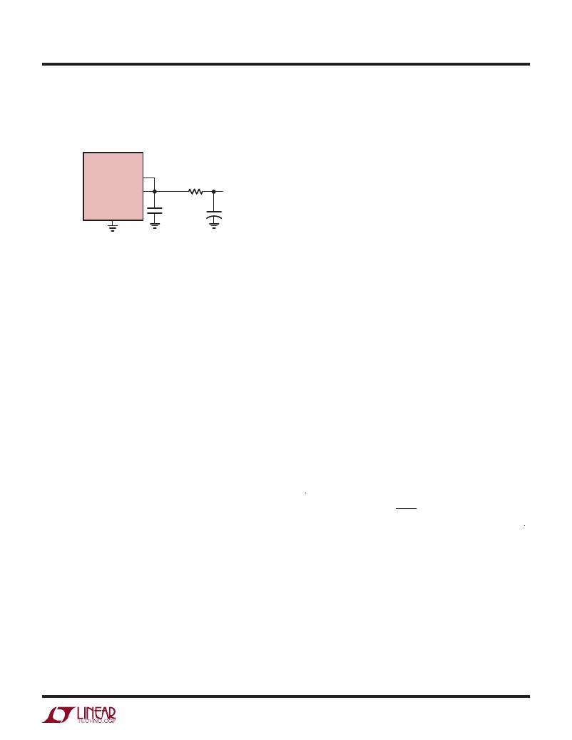
�LTC3855�
�INTV� CC� 5V�
�1?�
�4.7� μ� F�
�3855� F07�
�Figure� 10.� Setup� for� a� 5V� Input�
�Topside� MOSFET� Driver� Supply� (C� B� ,� DB)�
�External� bootstrap� capacitors� C� B� connected� to� the� BOOST�
�pins� supply� the� gate� drive� voltages� for� the� topside� MOSFETs.�
�Capacitor� C� B� in� the� Functional� Diagram� is� charged� though�
�external� diode� DB� from� INTV� CC� when� the� SW� pin� is� low.�
�When� one� of� the� topside� MOSFETs� is� to� be� turned� on,�
�the� driver� places� the� C� B� voltage� across� the� gate� source�
�of� the� desired� MOSFET.� This� enhances� the� MOSFET� and�
�turns� on� the� topside� switch.� The� switch� node� voltage,� SW,�
�rises� to� V� IN� and� the� BOOST� pin� follows.� With� the� topside�
�MOSFET� on,� the� boost� voltage� is� above� the� input� supply:�
�V� BOOST� =� V� IN� +� V� INTVCC� .� The� value� of� the� boost� capacitor�
�C� B� needs� to� be� 100� times� that� of� the� total� input� capa-�
�citance� of� the� topside� MOSFET(s).� The� reverse� break-�
�down� of� the� external� Schottky� diode� must� be� greater�
�than� V� IN(MAX)� .� When� adjusting� the� gate� drive� level,� the�
�final� arbiter� is� the� total� input� current� for� the� regulator.� If�
�a� change� is� made� and� the� input� current� decreases,� then�
�the� efficiency� has� improved.� If� there� is� no� change� in� input�
�current,� then� there� is� no� change� in� efficiency.�
�Undervoltage� Lockout�
�The� LTC3855� has� two� functions� that� help� protect� the�
�controller� in� case� of� undervoltage� conditions.� A� precision�
�UVLO� comparator� constantly� monitors� the� INTV� CC� voltage�
�to� ensure� that� an� adequate� gate-drive� voltage� is� present.� It�
�locks� out� the� switching� action� when� INTV� CC� is� below� 3.2V.�
�To� prevent� oscillation� when� there� is� a� disturbance� on� the�
�INTV� CC� ,� the� UVLO� comparator� has� 600mV� of� precision�
�hysteresis.�
�Another� way� to� detect� an� undervoltage� condition� is� to�
�monitor� the� V� IN� supply.� Because� the� RUN� pins� have� a�
�precision� turn-on� reference� of� 1.2V,� one� can� use� a� resistor�
�divider� to� V� IN� to� turn� on� the� IC� when� V� IN� is� high� enough.�
�An� extra� 4.5μA� of� current� flows� out� of� the� RUN� pin� once�
�the� RUN� pin� voltage� passes� 1.2V.� One� can� program� the�
�hysteresis� of� the� run� comparator� by� adjusting� the� values�
�of� the� resistive� divider.� For� accurate� V� IN� undervoltage�
�detection,� V� IN� needs� to� be� higher� than� 4.5V.�
�C� IN� and� C� OUT� Selection�
�The� selection� of� C� IN� is� simplified� by� the� 2-phase� architec-�
�ture� and� its� impact� on� the� worst-case� RMS� current� drawn�
�through� the� input� network� (battery/fuse/capacitor).� It� can� be�
�shown� that� the� worst-case� capacitor� RMS� current� occurs�
�when� only� one� controller� is� operating.� The� controller� with�
�the� highest� (V� OUT� )(I� OUT� )� product� needs� to� be� used� in� the�
�formula� below� to� determine� the� maximum� RMS� capacitor�
�current� requirement.� Increasing� the� output� current� drawn�
�from� the� other� controller� will� actually� decrease� the� input�
�RMS� ripple� current� from� its� maximum� value.� The� out-of-�
�phase� technique� typically� reduces� the� input� capacitor’s� RMS�
�ripple� current� by� a� factor� of� 30%� to� 70%� when� compared�
�to� a� single� phase� power� supply� solution.�
�In� continuous� mode,� the� source� current� of� the� top� MOSFET�
�is� a� square� wave� of� duty� cycle� (V� OUT� )/(V� IN� ).� To� prevent�
�large� voltage� transients,� a� low� ESR� capacitor� sized� for� the�
�maximum� RMS� current� of� one� channel� must� be� used.� The�
�maximum� RMS� capacitor� current� is� given� by:�
�1/2�
�V� IN�
�This� formula� has� a� maximum� at� V� IN� =� 2V� OUT� ,� where� I� RMS� =�
�I� OUT� /2.� This� simple� worst-case� condition� is� commonly� used�
�for� design� because� even� significant� deviations� do� not� of-�
�fer� much� relief.� Note� that� capacitor� manufacturers’� ripple�
�current� ratings� are� often� based� on� only� 2000� hours� of� life.�
�This� makes� it� advisable� to� further� derate� the� capacitor,� or�
�to� choose� a� capacitor� rated� at� a� higher� temperature� than�
�required.� Several� capacitors� may� be� paralleled� to� meet�
�size� or� height� requirements� in� the� design.� Due� to� the� high�
�operating� frequency� of� the� LTC3855,� ceramic� capacitors�
�3855f�
� �
�相关PDF资料 |
PDF描述 |
|---|---|
| VI-25K-EY-B1 | CONVERTER MOD DC/DC 40V 50W |
| LT3724IFE#TRPBF | IC REG CTRLR BST INV PWM 16TSSOP |
| VI-25K-EW-F4 | CONVERTER MOD DC/DC 40V 100W |
| LT3800IFE#TRPBF | IC REG CTRLR INV PWM CM 16-TSSOP |
| VI-25K-EW-F3 | CONVERTER MOD DC/DC 40V 100W |
相关代理商/技术参数 |
参数描述 |
|---|---|
| LTC3855IUJ#PBF | 功能描述:IC REG CTRLR BUCK PWM CM 40-QFN RoHS:是 类别:集成电路 (IC) >> PMIC - 稳压器 - DC DC 切换控制器 系列:PolyPhase® 特色产品:LM3753/54 Scalable 2-Phase Synchronous Buck Controllers 标准包装:1 系列:PowerWise® PWM 型:电压模式 输出数:1 频率 - 最大:1MHz 占空比:81% 电源电压:4.5 V ~ 18 V 降压:是 升压:无 回扫:无 反相:无 倍增器:无 除法器:无 Cuk:无 隔离:无 工作温度:-5°C ~ 125°C 封装/外壳:32-WFQFN 裸露焊盘 包装:Digi-Reel® 产品目录页面:1303 (CN2011-ZH PDF) 其它名称:LM3754SQDKR |
| LTC3855IUJ#PBF-ES | 制造商:Linear Technology 功能描述: |
| LTC3855IUJ#TRPBF | 功能描述:IC REG CTRLR BUCK PWM CM 40-QFN RoHS:是 类别:集成电路 (IC) >> PMIC - 稳压器 - DC DC 切换控制器 系列:PolyPhase® 标准包装:2,500 系列:- PWM 型:电流模式 输出数:1 频率 - 最大:500kHz 占空比:96% 电源电压:4 V ~ 36 V 降压:无 升压:是 回扫:无 反相:无 倍增器:无 除法器:无 Cuk:无 隔离:无 工作温度:-40°C ~ 125°C 封装/外壳:24-WQFN 裸露焊盘 包装:带卷 (TR) |
| LTC3856EFE#PBF | 功能描述:IC REG CTRLR BUCK PWM CM 38TFSOP RoHS:是 类别:集成电路 (IC) >> PMIC - 稳压器 - DC DC 切换控制器 系列:PolyPhase® 标准包装:2,000 系列:- PWM 型:电流模式 输出数:1 频率 - 最大:1MHz 占空比:50% 电源电压:9 V ~ 10 V 降压:无 升压:是 回扫:是 反相:无 倍增器:无 除法器:无 Cuk:无 隔离:无 工作温度:-40°C ~ 85°C 封装/外壳:8-TSSOP(0.173",4.40mm 宽) 包装:带卷 (TR) |
| LTC3856EFE#TRPBF | 功能描述:IC REG CTRLR BUCK PWM CM 38TSSOP RoHS:是 类别:集成电路 (IC) >> PMIC - 稳压器 - DC DC 切换控制器 系列:PolyPhase® 标准包装:2,500 系列:- PWM 型:电流模式 输出数:1 频率 - 最大:500kHz 占空比:96% 电源电压:4 V ~ 36 V 降压:无 升压:是 回扫:无 反相:无 倍增器:无 除法器:无 Cuk:无 隔离:无 工作温度:-40°C ~ 125°C 封装/外壳:24-WQFN 裸露焊盘 包装:带卷 (TR) |
发布紧急采购,3分钟左右您将得到回复。