- 您现在的位置:买卖IC网 > PDF目录9218 > LTC6946IUFD-2#PBF (Linear Technology)IC INTEGER-N PLL W/VCO 28-QFN PDF资料下载
参数资料
| 型号: | LTC6946IUFD-2#PBF |
| 厂商: | Linear Technology |
| 文件页数: | 14/30页 |
| 文件大小: | 0K |
| 描述: | IC INTEGER-N PLL W/VCO 28-QFN |
| 软件下载: | PLLWizard™ PLLWizard™, with .NET 2.0 installer |
| 标准包装: | 73 |
| 类型: | 时钟/频率合成器(RF/IF),分数-N,整数-N, |
| PLL: | 是 |
| 输入: | 时钟 |
| 输出: | 时钟 |
| 电路数: | 1 |
| 比率 - 输入:输出: | 1:1 |
| 差分 - 输入:输出: | 是/是 |
| 频率 - 最大: | 4.91GHz |
| 除法器/乘法器: | 是/是 |
| 电源电压: | 3.15 V ~ 5.25 V |
| 工作温度: | -40°C ~ 105°C |
| 安装类型: | 表面贴装 |
| 封装/外壳: | 28-WFQFN 裸露焊盘 |
| 供应商设备封装: | 28-QFN(4x5) |
| 包装: | 管件 |
第1页第2页第3页第4页第5页第6页第7页第8页第9页第10页第11页第12页第13页当前第14页第15页第16页第17页第18页第19页第20页第21页第22页第23页第24页第25页第26页第27页第28页第29页第30页
LTC6946
21
6946fa
APPLICATIONS INFORMATION
INTRODUCTION
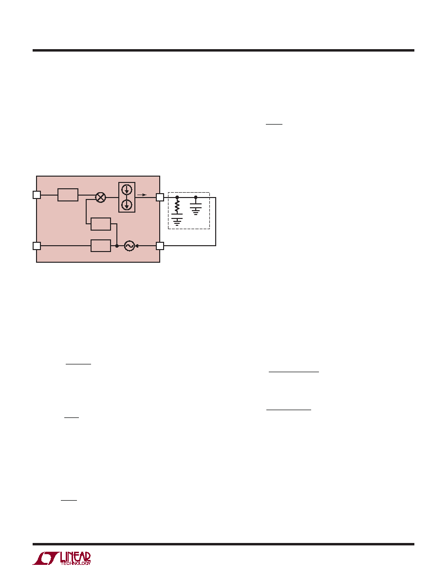
A PLL is a complex feedback system that may conceptually
be considered a frequency multiplier. The system multiplies
the frequency input at REF± and outputs a higher frequency
at RF±. The PFD, charge pump, N divider, and external VCO
and loop filter form a feedback loop to accurately control
the output frequency (see Figure 14). The R and O divider
are used to set the output frequency resolution.
Using the above equations, the output frequency resolu-
tion fSTEP produced by a unit change in N is given by
Equation 6:
fSTEP =
fREF
R O
(6)
LOOP FILTER DESIGN
A stable PLL system requires care in selecting the external
loop filter values. The Linear Technology PLLWizard ap-
plication, available from www.linear.com, aids in design
and simulation of the complete system.
The loop design should use the following algorithm:
1. Determine the output frequency, fRF, and frequency step
size, fSTEP, based on application requirements. Using
Equations 3, 4, 5 and 6, change fREF, N, R, and O until
the application frequency constraints are met. Use the
minimum R value that still satisfies the constraints.
Then calculate B using Equation 1 and Table 7.
2. Select the open-loop bandwidth, BW, constrained by
fPFD. A stable loop requires that BW is less than fPFD
by at least a factor of 10.
3. Select loop filter component RZ and charge pump cur-
rent ICP based on BW and the VCO gain factor, KVCO.
BW (in Hz) is approximated by the following equation:
BW
ICP RZ KVCO
2 π N
(7)
or
RZ =
2 π BW N
ICP KVCO
where KVCO is in Hz/V, ICP is in Amps, and RZ is in Ohms.
KVCO is obtained from the VCO tuning sensitivity in the
Electrical Characteristics. Use ICP = 11.2mA to lower in-
band noise unless component values force a lower setting.
R_DIV
N_DIV
÷R
÷N
O_DIV
÷O
fPFD
LTC6946
REF±
(fREF)
fVCO
KPFD
KVCO
25
RF±
(fRF)
15
CP
RZ
CI
CP
LOOP FILTER
LF(s)
6946 F14
TUNE
ICP
Figure 14. PLL Loop Diagram
OUTPUT FREQUENCY
When the loop is locked, the frequency fVCO (in Hz)
produced at the output of the VCO is determined by the
reference frequency, fREF, and the R and N divider values,
given by Equation 3:
fVCO =
fREF N
R
(3)
Here, the PFD frequency fPFD produced is given by the
following equation:
fPFD =
fREF
R
(4)
and fVCO may be alternatively expressed as:
fVCO = fPFD N
The output frequency fRF produced at the output of the O
divider is given by Equation 5:
fRF =
fVCO
O
(5)
相关PDF资料 |
PDF描述 |
|---|---|
| VI-B44-IU-B1 | CONVERTER MOD DC/DC 48V 200W |
| SY89429AJZ | IC SYNTHESIZER FREQ PROGR 28PLCC |
| SY58038UMY TR | IC MUX 8:1 PREC 1:2 LVPECL 44MLF |
| X9317WS8IZ-2.7 | IC XDCP SGL 100TAP 10K 8-SOIC |
| AD9514BCPZ | IC CLOCK DIST 3OUT PLL 32LFCSP |
相关代理商/技术参数 |
参数描述 |
|---|---|
| LTC6946IUFD-3#PBF | 功能描述:IC INTEGER-N PLL W/VCO 28-QFN RoHS:是 类别:集成电路 (IC) >> 时钟/计时 - 时钟发生器,PLL,频率合成器 系列:- 标准包装:2,000 系列:- 类型:PLL 频率合成器 PLL:是 输入:晶体 输出:时钟 电路数:1 比率 - 输入:输出:1:1 差分 - 输入:输出:无/无 频率 - 最大:1GHz 除法器/乘法器:是/无 电源电压:4.5 V ~ 5.5 V 工作温度:-20°C ~ 85°C 安装类型:表面贴装 封装/外壳:16-LSSOP(0.175",4.40mm 宽) 供应商设备封装:16-SSOP 包装:带卷 (TR) 其它名称:NJW1504V-TE1-NDNJW1504V-TE1TR |
| LTC6946IUFD-3#TRPBF | 功能描述:IC INTEGER-N PLL W/VCO 28QFN RoHS:是 类别:集成电路 (IC) >> 时钟/计时 - 时钟发生器,PLL,频率合成器 系列:- 标准包装:1,000 系列:Precision Edge® 类型:时钟/频率合成器 PLL:无 输入:CML,PECL 输出:CML 电路数:1 比率 - 输入:输出:2:1 差分 - 输入:输出:是/是 频率 - 最大:10.7GHz 除法器/乘法器:无/无 电源电压:2.375 V ~ 3.6 V 工作温度:-40°C ~ 85°C 安装类型:表面贴装 封装/外壳:16-VFQFN 裸露焊盘,16-MLF? 供应商设备封装:16-MLF?(3x3) 包装:带卷 (TR) 其它名称:SY58052UMGTRSY58052UMGTR-ND |
| LTC6946-x | 制造商:LINER 制造商全称:Linear Technology 功能描述:16-Bit, 20Msps Low Noise Dual ADC |
| LTC694C | 制造商:LINER 制造商全称:Linear Technology 功能描述:Microprocessor Supervisory Circuits |
| LTC694C-3.3 | 制造商:LINER 制造商全称:Linear Technology 功能描述:3.3V Microprocessor Supervisory Circuits |
发布紧急采购,3分钟左右您将得到回复。