- 您现在的位置:买卖IC网 > PDF目录69008 > LX1675ILQ-TR (MICROSEMI CORP-ANALOG MIXED SIGNAL GROUP) 1.5 A SWITCHING CONTROLLER, 690 kHz SWITCHING FREQ-MAX, PQCC38 PDF资料下载
参数资料
| 型号: | LX1675ILQ-TR |
| 厂商: | MICROSEMI CORP-ANALOG MIXED SIGNAL GROUP |
| 元件分类: | 稳压器 |
| 英文描述: | 1.5 A SWITCHING CONTROLLER, 690 kHz SWITCHING FREQ-MAX, PQCC38 |
| 封装: | 5 X 7 MM, ROHS COMPLIANT, PLASTIC, MLPQ-38 |
| 文件页数: | 14/19页 |
| 文件大小: | 324K |
| 代理商: | LX1675ILQ-TR |
LX1675
PRODUCTION DATA SHEET
Microsemi
Integrated Products Division
11861 Western Avenue, Garden Grove, CA. 92841, 714-898-8121, Fax: 714-893-2570
Page 4
Copyright
2004
Rev. 1.2a, 2006-02-16
WWW
.Microse
m
i
.CO
M
Multiple Output LoadSHARE PWM
TM
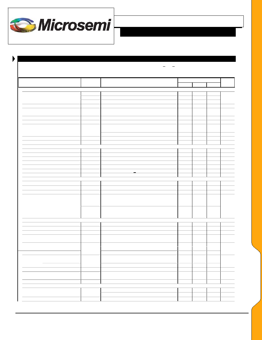
ELECTRICAL CHA RACTERISTICS
For the LX1675ILQ the following specifications apply over the ambient temperature -40°C < TA < 85°C and for the LX1675CLQ 0
°C
≤
TA ≤ 85°C except where otherwise noted and the following test conditions: VIN & VSLR = 12V, VCX = 17V, HOX and LOX =3000pF
Load, FS = 0 (f = 300KHz).
LX1675
Parameter
Symbol
Test Conditions
Min
Typ
Max
Units
SWITCHING REGULATORS
VIN
Regulator Functional
4.5
24
VCX
30
Input Voltage
VCCL
6
V
Operation Current
IVIN
Static
6
mA
Feedback Voltage Internal
Reference
VFB
4.5V < VIN < 12V
0.784
0.816
V
Line Regulation
-1
1
%
Load Regulation
System Level measurement, Closed Loop
-1
1
%
High Side Minimum Pulse Width
Load = 3000pF
50
nS
600kHz
74
%
Maximum Duty Cycle
PWMDC
85
%
Lox Minimum On Time
VLOx
@ 25°C from 3V going high to 1V going low
180
225
320
nS
Buffered Reference Voltage
VREF
Max Load Current 0.5mA
0.778
0.822
V
ERROR AMPLIFIER
Input Offset Voltage
VOS
Common Mode Input Voltage = 1V
-7.0
7.0
mV
DC Open Loop Gain
70
dB
Unity gain bandwidth
AVUGBW
10
MHz
High Output Voltage
VOH
I Source = 2mA
3.75
5.0
V
Low Output Voltage
VOL
I Sink = 100A
100
mV
Input Common Mode Range
Input Offset Voltage < 20mV
0.1
3.5
V
Input Bias Current
IIN
0V and 3.5V Common Mode Voltage
100
nA
CURRENT SENSE
CS Bias Current (Source)
ISET
VCSX = -0.2V, VPGX = 0V @ 25°C
48
55
62
A
CS Trip Threshold
VTRIP
Referenced to VCSX, VPGX = 0V
±3
mV
CS Delay (Blanking)
TCSD
150
nS
VIH
Any PWM Output Activating Current Limit for
More than 4 Clock Cycles, Soft Starts all PWM
Outputs
2
Shared Fault Mode
VIL
Current Limit Event of One PWM Does Not Effect
the Continued Function of the Two Other PWM
Regulators
0.8
V
OUTPUT DRIVERS – N Channel MOSFETS
Low Side Driver Operating Current
IVCCL
Static
2.5
mA
High Side Driver Operating Current
IVCX
Static
3
mA
Drive Rise and Fall Time
TR/F
CL = 3000pF
50
nS
Dead Time – High Side to Low Side
or Low Side to High Side
TDEAD
Drive Load = 3000pF, VDRIVE < 1V
50
nS
High Side Driver Voltage
Drive High
IHOx = 20mA, VCx – HRx = 5.0V
4.8
4.9
Drive Low
VHOx
IHOx = -20mA, VCx – HRx = 5.0V
0.1
0.2
V
Low Side Driver Voltage
Drive High
ILOx = 20mA, VCCL – PGx = 5.0V
4.8
4.9
Drive Low
VLOx
ILOx = -20mA, VCCL – PGx = 5.0V
0.1
0.2
V
High Side Driver Current
IHOx
VCx – HRx = 5.0V, Capacitive Load, PW < 200ns
±1
APEAK
Low Side Driver Current
ILOx
VCCL – PGx = 5.0V, Capacitive Load, PW <
200ns
±1.5
APEAK
Maximum Load
QgMAX
50
nC
OSCILLATOR
VFS <0.8V @ 25°C
255
300
345
KHz
PWM Switching Frequency
FSW
VFS >2V @ 25°C
510
600
690
KHz
Ramp Amplitude
VRAMP
1.6
VPP
EE
LL
EE
CC
TT
RR
IICC
AA
LL
SS
相关PDF资料 |
PDF描述 |
|---|---|
| LX1675CLQ-TR | 1.5 A SWITCHING CONTROLLER, 690 kHz SWITCHING FREQ-MAX, PQCC38 |
| LX1684CDT | 1 A SWITCHING CONTROLLER, 200 kHz SWITCHING FREQ-MAX, PDSO14 |
| LX1689CPW-TR | FLUORESCENT LIGHT CONTROLLER, 500 kHz SWITCHING FREQ-MAX, PDSO20 |
| LX1689IPW-TR | FLUORESCENT LIGHT CONTROLLER, 500 kHz SWITCHING FREQ-MAX, PDSO20 |
| LX1691IPWTR | 0.1 A FLUORESCENT LIGHT CONTROLLER, 250 kHz SWITCHING FREQ-MAX, PDSO16 |
相关代理商/技术参数 |
参数描述 |
|---|---|
| LX1676 | 制造商:MICROSEMI 制造商全称:Microsemi Corporation 功能描述:Mobile AMD Athlon? VRM Controller |
| LX1676 EVAL KIT | 制造商:Microsemi Corporation 功能描述:PWM CONTROLLERS - Bulk |
| LX1676_05 | 制造商:MICROSEMI 制造商全称:Microsemi Corporation 功能描述:Mobile AMD Athlon? VRM Controller |
| LX1676CLQ | 功能描述:IC CTRLR PS VRM BIPHASE 38MLPQ RoHS:是 类别:集成电路 (IC) >> PMIC - 稳压器 - 专用型 系列:- 标准包装:2,000 系列:- 应用:控制器,DSP 输入电压:4.5 V ~ 25 V 输出数:2 输出电压:最低可调至 1.2V 工作温度:-40°C ~ 85°C 安装类型:表面贴装 封装/外壳:30-TFSOP(0.173",4.40mm 宽) 供应商设备封装:30-TSSOP 包装:带卷 (TR) |
| LX1676-CLQ | 制造商:MICROSEMI 制造商全称:Microsemi Corporation 功能描述:Mobile AMD AthlonTM VRM Controller |
发布紧急采购,3分钟左右您将得到回复。