- 您现在的位置:买卖IC网 > PDF目录180051 > M-ORT82G51BM680-DB (LATTICE SEMICONDUCTOR CORP) FPGA, 1296 CLBS, 333000 GATES, PBGA680 PDF资料下载
参数资料
| 型号: | M-ORT82G51BM680-DB |
| 厂商: | LATTICE SEMICONDUCTOR CORP |
| 元件分类: | FPGA |
| 英文描述: | FPGA, 1296 CLBS, 333000 GATES, PBGA680 |
| 封装: | PLASTIC, FBGA-680 |
| 文件页数: | 7/94页 |
| 文件大小: | 2104K |
| 代理商: | M-ORT82G51BM680-DB |
第1页第2页第3页第4页第5页第6页当前第7页第8页第9页第10页第11页第12页第13页第14页第15页第16页第17页第18页第19页第20页第21页第22页第23页第24页第25页第26页第27页第28页第29页第30页第31页第32页第33页第34页第35页第36页第37页第38页第39页第40页第41页第42页第43页第44页第45页第46页第47页第48页第49页第50页第51页第52页第53页第54页第55页第56页第57页第58页第59页第60页第61页第62页第63页第64页第65页第66页第67页第68页第69页第70页第71页第72页第73页第74页第75页第76页第77页第78页第79页第80页第81页第82页第83页第84页第85页第86页第87页第88页第89页第90页第91页第92页第93页第94页
Lattice Semiconductor
ORCA ORT82G5 Data Sheet
15
logic and record status. These bits are passed to the core using the FPGA System Bus and are described in later
sections of this data sheet Table 8.
The low-speed transmit interface consists of a clock and 4 data bytes, each with an accompanying control bit. The
data bytes are conveyed to the MUX via the TWDxx[31:0] ports (where xx represents the channel label [AA,...,BD]).
The control bits are TCOMMAx[3:0] which dene whether the input byte is to be interpreted as data or as a special
character and TBIT9xx[3:0] which are used to force negative disparity encoding. The data and control signals are
synchronized to the transmit clock, TSYS_CLK_xx. Both the data and control are strobed into the core on the rising
edge of TSYS_CLK_xx.
The MUX is responsible for taking 40 bits of data/control at the low-speed transmit interface and up-converting it to
10 bits of data/control at the SERDES transmit interface. The MUX has 2 clock domains - one based on the clock
received from the SERDES block and a second that comes from the FPGA at 1/4 the frequency of the SERDES
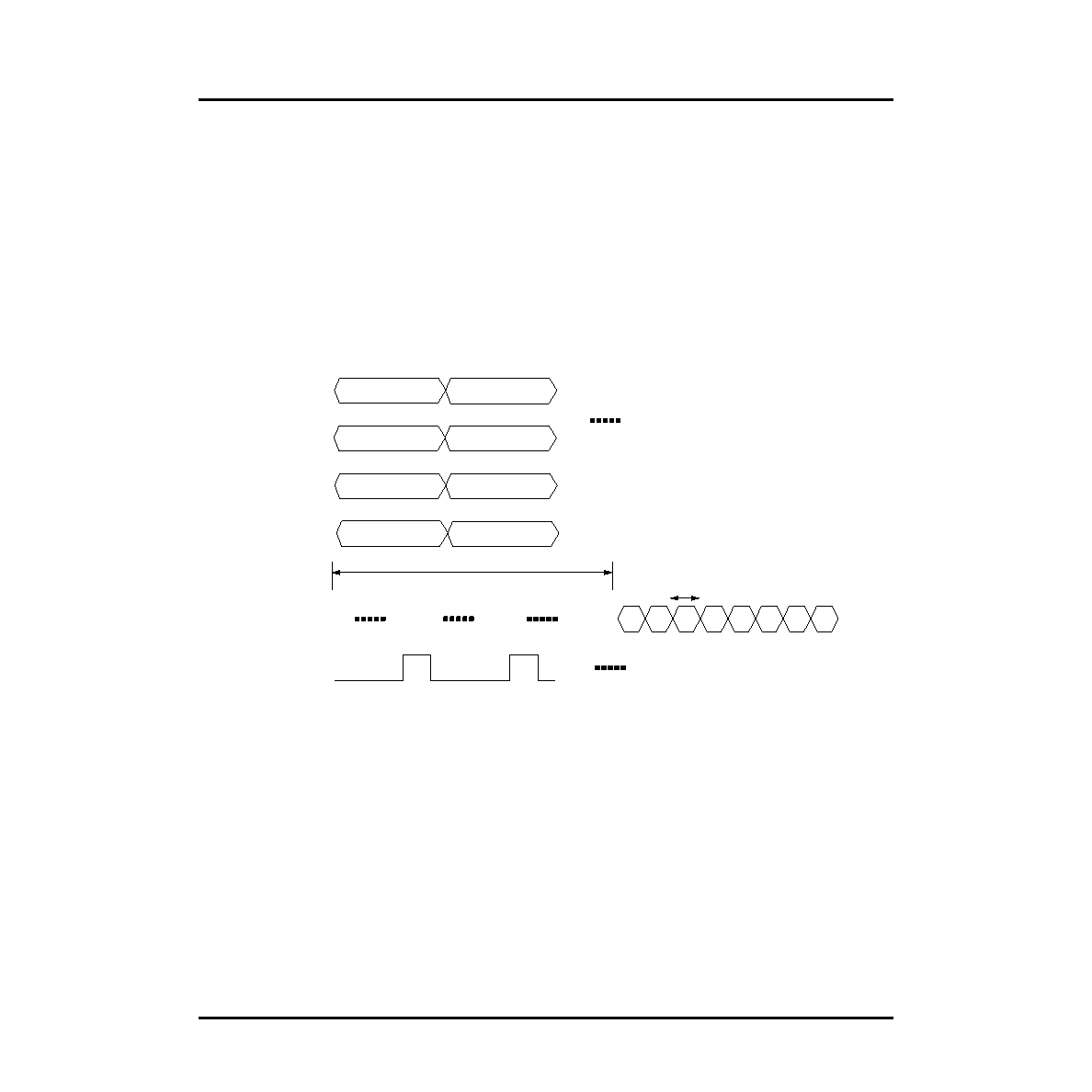
clock. The time sequence of interleaving data/control values is shown in Figure 4 below.
Figure 4. Transmit MUX Block Timing - Single Channel
SERDES Block
The SERDES block accepts either 8-bit unencoded data or 10-bit encoded data at the parallel input port from the
MUX/DEMUX block. It also accepts the reference clock at the REFCLK_[A:B] input and uses this clock to synthe-
size the internal high-speed serial bit clock.
The internal STBC311xx clock is derived from the reference clock. The frequency of this clock depends on the set-
ting of the half-rate/full-rate control bit setting the mode of the SERDES and the frequency of the REFCLK_[A:B]
and/or that of the high-speed serial data. A falling edge on the STBC311xx clock port will cause a new data charac-
ter to be transferred into the SERDES block. The latency from the SERDES block input to the high-speed serial
output is 5 STBC311xx clock cycles, as shown in Figure 5.
pq
r
s
t
xyz
STBDxx[9:0]
LATENCY = 4 TSYS_CLK_xx CLOCKS
TWDxx[31:24],
TSYS_CLK_xx
s
8
r
8
z
8
y
8
10-bit wide data
TWDxx[23:16],
TWDxx[15:8],
r
7-0,
y
7-0,
TCOMMAxx[3]
TCOMMAxx[2]
TCOMMAxx[1]
TCOMMAxx[0]
TWDxx[7:0],
s
7-0,
z
7-0,
TBIT9xx[0]
TBIT9xx[1]
TBIT9xx[2]
TBIT9xx[3]
q
9
r
9
s
9
z
9
y
9
x
9
p
7-0,
p
8
t
7-0,
q
8
t
8
x
8
q
7-0,
x
7-0,
p
9
t
9
相关PDF资料 |
PDF描述 |
|---|---|
| M-ORT82G52BM680-DB | FPGA, 1296 CLBS, 333000 GATES, PBGA680 |
| M.PI-1R1D12 | 1 ELEMENT, 1.1 uH, GENERAL PURPOSE INDUCTOR, SMD |
| M01-014-1452PA | 14 CONTACT(S), MALE, RIGHT ANGLE TELECOM AND DATACOM CONNECTOR, SOLDER |
| M01-016-1443PA | 16 CONTACT(S), MALE, RIGHT ANGLE TELECOM AND DATACOM CONNECTOR, SOLDER |
| M0302CS-9N2XJSU | 1 ELEMENT, 0.0092 uH, CERAMIC-CORE, GENERAL PURPOSE INDUCTOR, SMD |
相关代理商/技术参数 |
参数描述 |
|---|---|
| MORTAR-44LB | 制造商:3M Electronic Products Division 功能描述:3M(TM) FIRE BARRIER MORTAR, 44 98040056073 制造商:3M Electronic Products Division 功能描述:Fire Barrier 44 lb Bag |
| MO-RX3930 | 制造商:未知厂家 制造商全称:未知厂家 功能描述:FSK RECEIVER MODULE |
| MO-RX3930-FS | 制造商:未知厂家 制造商全称:未知厂家 功能描述:FSK RECEIVER MODULE |
| MO-RX3930-FS315M | 制造商:未知厂家 制造商全称:未知厂家 功能描述:FSK RECEIVER MODULE |
| MO-RX3930-FS434M | 制造商:未知厂家 制造商全称:未知厂家 功能描述:FSK RECEIVER MODULE |
发布紧急采购,3分钟左右您将得到回复。