- 您现在的位置:买卖IC网 > PDF目录377808 > M28W160CB100N6T (意法半导体) 16 Mbit (1Mb x16, Boot Block) 3V Supply Flash Memory PDF资料下载
参数资料
| 型号: | M28W160CB100N6T |
| 厂商: | 意法半导体 |
| 英文描述: | 16 Mbit (1Mb x16, Boot Block) 3V Supply Flash Memory |
| 中文描述: | 16兆位(1兆x16插槽,引导块)3V电源快闪记忆体 |
| 文件页数: | 38/50页 |
| 文件大小: | 327K |
| 代理商: | M28W160CB100N6T |
第1页第2页第3页第4页第5页第6页第7页第8页第9页第10页第11页第12页第13页第14页第15页第16页第17页第18页第19页第20页第21页第22页第23页第24页第25页第26页第27页第28页第29页第30页第31页第32页第33页第34页第35页第36页第37页当前第38页第39页第40页第41页第42页第43页第44页第45页第46页第47页第48页第49页第50页
M28W160CT, M28W160CB
38/50
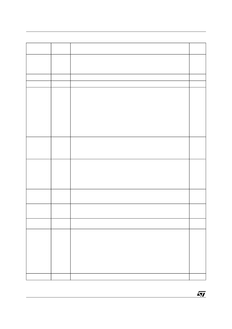
Table 30. Primary Algorithm-Specific Extended Query Table
Note: 1. See Table 27, offset 15 for P pointer definition.
Offset
P = 35h
(1)
Data
Description
Value
(P+0)h = 35h
0050h
Primary Algorithm extended Query table unique ASCII string “PRI”
"P"
(P+1)h = 36h
0052h
"R"
(P+2)h = 37h
0049h
"I"
(P+3)h = 38h
0031h
Major version number, ASCII
"1"
(P+4)h = 39h
0030h
Minor version number, ASCII
"0"
(P+5)h = 3Ah
0066h
Extended Query table contents for Primary Algorithm. Address (P+5)h
contains less significant byte.
bit 0
Chip Erase supported
bit 1
Suspend Erase supported
bit 2
Suspend Program supported
bit 3
Legacy Lock/Unlock supported
bit 4
Queued Erase supported
bit 5
Instant individual block locking supported (1 = Yes, 0 = No)
bit 6
Protection bits supported
bit 7
Page mode read supported
bit 8
Synchronous read supported
bit 31 to 9
Reserved; undefined bits are ‘0’
(1 = Yes, 0 = No)
(1 = Yes, 0 = No)
(1 = Yes, 0 = No)
(1 = Yes, 0 = No)
(1 = Yes, 0 = No)
(1 = Yes, 0 = No)
(1 = Yes, 0 = No)
(1 = Yes, 0 = No)
No
Yes
Yes
No
No
Yes
Yes
No
No
(P+6)h = 3Bh
0000h
(P+7)h = 3Ch
0000h
(P+8)h = 3Dh
0000h
(P+9)h = 3Eh
0001h
Supported Functions after Suspend
Read Array, Read Status Register and CFI Query are always supported
during Erase or Program operation
bit 0
Program supported after Erase Suspend (1 = Yes, 0 = No)
bit 7 to 1
Reserved; undefined bits are ‘0’
Yes
(P+A)h = 3Fh
0003h
Block Lock Status
Defines which bits in the Block Status Register section of the Query are
implemented.
Address (P+A)h contains less significant byte
bit 0
Block Lock Status Register Lock/Unlock bit active(1 = Yes, 0 = No)
bit 1
Block Lock Status Register Lock-Down bit active (1 = Yes, 0 = No)
bit 15 to 2
Reserved for future use; undefined bits are ‘0’
Yes
Yes
(P+B)h = 40h
0000h
(P+C)h = 41h
0030h
V
DD
Logic Supply Optimum Program/Erase voltage (highest performance)
bit 7 to 4
HEX value in volts
bit 3 to 0
BCD value in 100 mV
3V
(P+D)h = 42h
00C0h
V
PP
Supply Optimum Program/Erase voltage
bit 7 to 4
HEX value in volts
bit 3 to 0
BCD value in 100 mV
12V
(P+E)h = 43h
0001h
Number of Protection register fields in JEDEC ID space.
"00h," indicates that 256 protection bytes are available
01
(P+F)h = 44h
0080h
Protection Field 1: Protection Description
This field describes user-available. One Time Programmable (OTP)
Protection register bytes. Some are pre-programmed with device unique
serial numbers. Others are user programmable. Bits 0–15 point to the
Protection register Lock byte, the section’s first byte.
The following bytes are factory pre-programmed and user-programmable.
bit 0 to 7
Lock/bytes JEDEC-plane physical low address
bit 8 to 15
Lock/bytes JEDEC-plane physical high address
bit 16 to 23 "n" such that 2
n
= factory pre-programmed bytes
bit 24 to 31 "n" such that 2
n
= user programmable bytes
80h
(P+10)h = 45h
0000h
00h
(P+11)h = 46h
0003h
8 Byte
(P+12)h = 47h
0003h
8 Byte
(P+13)h = 48h
Reserved
相关PDF资料 |
PDF描述 |
|---|---|
| M28W160CB85ZB6E | 16 Mbit (1Mb x16, Boot Block) 3V Supply Flash Memory |
| M28W160CB85ZB6F | 16 Mbit (1Mb x16, Boot Block) 3V Supply Flash Memory |
| M28W160CB85ZB6S | 16 Mbit (1Mb x16, Boot Block) 3V Supply Flash Memory |
| M28W160CB85ZB6T | 16 Mbit (1Mb x16, Boot Block) 3V Supply Flash Memory |
| M28W160CB85ZB6U | 16 Mbit (1Mb x16, Boot Block) 3V Supply Flash Memory |
相关代理商/技术参数 |
参数描述 |
|---|---|
| M28W160CB100N6U | 制造商:NUMONYX 制造商全称:Numonyx B.V 功能描述:16 Mbit (1Mb x16, Boot Block) 3V Supply Flash Memory |
| M28W160CB100ZB1 | 制造商:NUMONYX 制造商全称:Numonyx B.V 功能描述:16 Mbit (1Mb x16, Boot Block) 3V Supply Flash Memory |
| M28W160CB100ZB1E | 制造商:NUMONYX 制造商全称:Numonyx B.V 功能描述:16 Mbit (1Mb x16, Boot Block) 3V Supply Flash Memory |
| M28W160CB100ZB1F | 制造商:NUMONYX 制造商全称:Numonyx B.V 功能描述:16 Mbit (1Mb x16, Boot Block) 3V Supply Flash Memory |
| M28W160CB100ZB1S | 制造商:NUMONYX 制造商全称:Numonyx B.V 功能描述:16 Mbit (1Mb x16, Boot Block) 3V Supply Flash Memory |
发布紧急采购,3分钟左右您将得到回复。