- 您现在的位置:买卖IC网 > PDF目录296349 > M29F800DB90N6T (NUMONYX) 512K X 16 FLASH 5V PROM, 70 ns, PDSO48 PDF资料下载
参数资料
| 型号: | M29F800DB90N6T |
| 厂商: | NUMONYX |
| 元件分类: | PROM |
| 英文描述: | 512K X 16 FLASH 5V PROM, 70 ns, PDSO48 |
| 封装: | 12 X 20 MM, PLASTIC, TSOP-48 |
| 文件页数: | 35/39页 |
| 文件大小: | 622K |
| 代理商: | M29F800DB90N6T |
第1页第2页第3页第4页第5页第6页第7页第8页第9页第10页第11页第12页第13页第14页第15页第16页第17页第18页第19页第20页第21页第22页第23页第24页第25页第26页第27页第28页第29页第30页第31页第32页第33页第34页当前第35页第36页第37页第38页第39页
5/39
SUMMARY DESCRIPTION
The M29F800D is a 8 Mbit (1Mb x8 or 512Kb x16)
non-volatile memory that can be read, erased and
reprogrammed. These operations can be per-
formed using a single low voltage (5V) supply. On
power-up the memory defaults to its Read mode
where it can be read in the same way as a ROM or
EPROM.
The memory is divided into blocks that can be
erased independently so it is possible to preserve
valid data while old data is erased. Each block can
be protected independently to prevent accidental
Program or Erase commands from modifying the
memory. Program and Erase commands are writ-
ten to the Command Interface of the memory. An
on-chip Program/Erase Controller simplifies the
process of programming or erasing the memory by
taking care of all of the special operations that are
required to update the memory contents.
The end of a program or erase operation can be
detected and any error conditions identified. The
command set required to control the memory is
consistent with JEDEC standards.
The blocks in the memory are asymmetrically ar-
The first or last 64 Kbytes have been divided into
four additional blocks. The 16 Kbyte Boot Block
can be used for small initialization code to start the
microprocessor, the two 8 Kbyte Parameter
Blocks can be used for parameter storage and the
remaining 32K is a small Main Block where the ap-
plication may be stored.
Chip Enable, Output Enable and Write Enable sig-
nals control the bus operation of the memory.
They allow simple connection to most micropro-
cessors, often without additional logic.
The memory is offered in SO44 and TSOP48 (12
x 20mm) packages. The memory is supplied with
all the bits erased (set to ’1’).
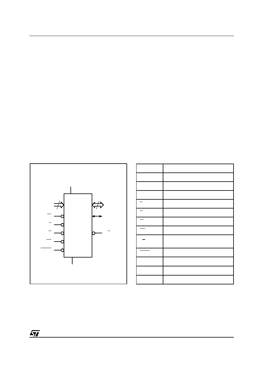
Figure 2. Logic Diagram
Table 1. Signal Names
AI06148B
19
A0-A18
W
DQ0-DQ14
VCC
M29F800DT
M29F800DB
E
VSS
15
G
RP
DQ15A–1
RB
BYTE
A0-A18
Address Inputs
DQ0-DQ7
Data Inputs/Outputs
DQ8-DQ14
Data Inputs/Outputs
DQ15A–1
Data Input/Output or Address Input
E
Chip Enable
G
Output Enable
W
Write Enable
RP
Reset/Block Temporary Unprotect
RB
Ready/Busy Output
(not available on SO44 package)
BYTE
Byte/Word Organization Select
VCC
Supply Voltage
VSS
Ground
NC
Not Connected Internally
相关PDF资料 |
PDF描述 |
|---|---|
| M29W160BT90ZA6 | 1M X 16 FLASH 2.7V PROM, 90 ns, PBGA48 |
| M29W400BT70M6T | 256K X 16 FLASH 2.7V PROM, 70 ns, PDSO44 |
| M29W640GB70ZA6F | 4M X 16 FLASH 3V PROM, 70 ns, PBGA48 |
| M2Y51264TU88A2G-37B | 64M X 64 DDR DRAM MODULE, 0.5 ns, DMA240 |
| M30-1201100 | 22 CONTACT(S), FEMALE, TWO PART BOARD CONNECTOR, CRIMP |
相关代理商/技术参数 |
参数描述 |
|---|---|
| M29F800DT55M1 | 功能描述:闪存 SO-44 1MX8/512KX16 RoHS:否 制造商:ON Semiconductor 数据总线宽度:1 bit 存储类型:Flash 存储容量:2 MB 结构:256 K x 8 定时类型: 接口类型:SPI 访问时间: 电源电压-最大:3.6 V 电源电压-最小:2.3 V 最大工作电流:15 mA 工作温度:- 40 C to + 85 C 安装风格:SMD/SMT 封装 / 箱体: 封装:Reel |
| M29F800DT55N1 | 功能描述:闪存 1Mx8 or 512Kx16 55ns RoHS:否 制造商:ON Semiconductor 数据总线宽度:1 bit 存储类型:Flash 存储容量:2 MB 结构:256 K x 8 定时类型: 接口类型:SPI 访问时间: 电源电压-最大:3.6 V 电源电压-最小:2.3 V 最大工作电流:15 mA 工作温度:- 40 C to + 85 C 安装风格:SMD/SMT 封装 / 箱体: 封装:Reel |
| M29F800DT55N6 | 功能描述:闪存 1Mx8 or 512Kx16 55ns RoHS:否 制造商:ON Semiconductor 数据总线宽度:1 bit 存储类型:Flash 存储容量:2 MB 结构:256 K x 8 定时类型: 接口类型:SPI 访问时间: 电源电压-最大:3.6 V 电源电压-最小:2.3 V 最大工作电流:15 mA 工作温度:- 40 C to + 85 C 安装风格:SMD/SMT 封装 / 箱体: 封装:Reel |
| M29F800DT55N6E | 功能描述:闪存 STD FLASH 8 MEG RoHS:否 制造商:ON Semiconductor 数据总线宽度:1 bit 存储类型:Flash 存储容量:2 MB 结构:256 K x 8 定时类型: 接口类型:SPI 访问时间: 电源电压-最大:3.6 V 电源电压-最小:2.3 V 最大工作电流:15 mA 工作温度:- 40 C to + 85 C 安装风格:SMD/SMT 封装 / 箱体: 封装:Reel |
| M29F800DT70M1 | 功能描述:闪存 1Mx8 or 512Kx16 70ns RoHS:否 制造商:ON Semiconductor 数据总线宽度:1 bit 存储类型:Flash 存储容量:2 MB 结构:256 K x 8 定时类型: 接口类型:SPI 访问时间: 电源电压-最大:3.6 V 电源电压-最小:2.3 V 最大工作电流:15 mA 工作温度:- 40 C to + 85 C 安装风格:SMD/SMT 封装 / 箱体: 封装:Reel |
发布紧急采购,3分钟左右您将得到回复。