- 您现在的位置:买卖IC网 > PDF目录80479 > M37542F8VGP 8-BIT, FLASH, 8 MHz, MICROCONTROLLER, PQFP32 PDF资料下载
参数资料
| 型号: | M37542F8VGP |
| 元件分类: | 微控制器/微处理器 |
| 英文描述: | 8-BIT, FLASH, 8 MHz, MICROCONTROLLER, PQFP32 |
| 封装: | 7 X 7 MM, 0.80 MM PITCH, PLASTIC, LQFP-32 |
| 文件页数: | 11/139页 |
| 文件大小: | 1448K |
| 代理商: | M37542F8VGP |
第1页第2页第3页第4页第5页第6页第7页第8页第9页第10页当前第11页第12页第13页第14页第15页第16页第17页第18页第19页第20页第21页第22页第23页第24页第25页第26页第27页第28页第29页第30页第31页第32页第33页第34页第35页第36页第37页第38页第39页第40页第41页第42页第43页第44页第45页第46页第47页第48页第49页第50页第51页第52页第53页第54页第55页第56页第57页第58页第59页第60页第61页第62页第63页第64页第65页第66页第67页第68页第69页第70页第71页第72页第73页第74页第75页第76页第77页第78页第79页第80页第81页第82页第83页第84页第85页第86页第87页第88页第89页第90页第91页第92页第93页第94页第95页第96页第97页第98页第99页第100页第101页第102页第103页第104页第105页第106页第107页第108页第109页第110页第111页第112页第113页第114页第115页第116页第117页第118页第119页第120页第121页第122页第123页第124页第125页第126页第127页第128页第129页第130页第131页第132页第133页第134页第135页第136页第137页第138页第139页
7542 Group
Rev.3.02
Oct 31, 2006
Page 108 of 134
REJ03B0006-0302
Electrical Characteristics (Extended operating temperature version)
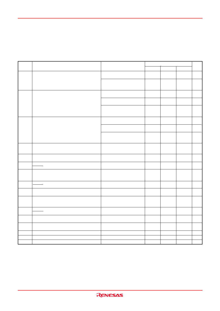
Table 31 Electrical characteristics (1) (Extended operating temperature version)
(FLASH ROM version: VCC = 2.7 to 5.5V, Mask ROM version: VCC = 2.4 to 5.5 V, VSS = 0 V, Ta = –40 to 85 °C, unless otherwise noted)
Min.
Typ.
Max.
Symbol
Parameter
Limits
Unit
IOH = –5 mA
VCC = 4.0 to 5.5 V
IOH = –1.0 mA
Mask ROM: VCC = 2.4 to 5.5 V
FLASH ROM: VCC = 2.7 to 5.5 V
IOL = 5 mA
VCC = 4.0 to 5.5 V
IOL = 1.5 mA
VCC = 4.0 to 5.5 V
IOL = 1.0 mA
Mask ROM: VCC = 2.4 to 5.5 V
FLASH ROM: VCC = 2.7 to 5.5 V
IOL = 15 mA
VCC = 4.0 to 5.5 V
IOL = 1.5 mA
VCC = 4.0 to 5.5 V
IOL = 1.0 mA
Mask ROM: VCC = 2.4 to 5.5 V
FLASH ROM: VCC = 2.7 to 5.5 V
VI = VCC
(Pin floating. Pull up transistors
“off”)
VI = VCC
VI = VSS
(Pin floating. Pull up transistors
“off”)
VI = VSS
(Pull up transistors “on”)
When clock stopped
VCC = 5.0 V, Ta = 25 °C
Test conditions
VCC–1.5
VCC–1.0
2.0
1000
62.5
“H” output voltage
P00–P07, P10–P14, P20–P27, P30–P37 (Note 1)
“L” output voltage
P00–P07, P30–P37 (Drive capacity = “L”)
P10–P14, P20–P27
“L” output voltage
P00–P07, P30–P37 (Drive capacity = “H”)
Hysteresis
CNTR0, INT0, INT1, CAP0, CAP1 (Note 2)
P00–P07 (Note 3)
Hysteresis
RXD0, SCLK0, RXD1, SCLK1
Hysteresis
RESET
“H” input current
P00–P07, P10–P14, P20–P27, P30–P37
“H” input current
RESET
“H” input current
XIN
“L” input current
P00–P07, P10–P14, P20–P27, P30–P37
“L” input current
RESET
“L” input current
XIN
“L” input current
P00–P07, P30–P37
RAM hold voltage
On-chip oscillator oscillation frequency
Oscillation stop detection circuit detection frequency
1.5
0.3
1.0
2.0
0.3
1.0
5.0
–5.0
–0.5
5.5
3000
187.5
V
A
mA
V
kHz
VOH
VOL
VT+–VT–
IIH
IIL
VRAM
ROSC
DOSC
0.4
0.5
4.0
–4.0
–0.2
2000
125
Notes 1: P11 is measured when the P11/TXD1 P-channel output disable bit of the UART1 control register (bit 4 of address 001B16) is “0”.
2: RXD1, SCLK1, INT0, and INT1 (P36 selected) have hysteresises only when bits 0 to 2 of the port P1P3 control register are set to “0” (CMOS level).
3: It is available only when operating key-on wake up.
相关PDF资料 |
PDF描述 |
|---|---|
| M30620FCPFP | 16-BIT, FLASH, 24 MHz, MICROCONTROLLER, PQFP100 |
| MB90F342CSPF | 16-BIT, FLASH, 24 MHz, MICROCONTROLLER, PQFP100 |
| MC9S12C32VFA25 | 16-BIT, FLASH, 25 MHz, MICROCONTROLLER, PQFP48 |
| MSC1200Y2PFBT | 8-BIT, FLASH, 33 MHz, MICROCONTROLLER, PQFP48 |
| MC68HC11E1VFN3R2 | 8-BIT, 3 MHz, MICROCONTROLLER, PQCC52 |
相关代理商/技术参数 |
参数描述 |
|---|---|
| M37542M2-XXXFP | 制造商:RENESAS 制造商全称:Renesas Technology Corp 功能描述:SINGLE-CHIP 8-BIT CMOS MICROCOMPUTER |
| M37542M2-XXXGP | 制造商:RENESAS 制造商全称:Renesas Technology Corp 功能描述:SINGLE-CHIP 8-BIT CMOS MICROCOMPUTER |
| M37542M2-XXXHP | 制造商:RENESAS 制造商全称:Renesas Technology Corp 功能描述:SINGLE-CHIP 8-BIT CMOS MICROCOMPUTER |
| M37542M2-XXXSP | 制造商:RENESAS 制造商全称:Renesas Technology Corp 功能描述:SINGLE-CHIP 8-BIT CMOS MICROCOMPUTER |
| M37542M4-XXXFP | 制造商:RENESAS 制造商全称:Renesas Technology Corp 功能描述:SINGLE-CHIP 8-BIT CMOS MICROCOMPUTER |
发布紧急采购,3分钟左右您将得到回复。