- 您现在的位置:买卖IC网 > PDF目录132980 > M37545G4-XXXGP 8-BIT, MROM, 4 MHz, MICROCONTROLLER, PQFP32 PDF资料下载
参数资料
| 型号: | M37545G4-XXXGP |
| 元件分类: | 微控制器/微处理器 |
| 英文描述: | 8-BIT, MROM, 4 MHz, MICROCONTROLLER, PQFP32 |
| 封装: | 7 X 7 MM, 0.80 MM PITCH, PLASTIC, LQFP-32 |
| 文件页数: | 59/65页 |
| 文件大小: | 782K |
| 代理商: | M37545G4-XXXGP |
第1页第2页第3页第4页第5页第6页第7页第8页第9页第10页第11页第12页第13页第14页第15页第16页第17页第18页第19页第20页第21页第22页第23页第24页第25页第26页第27页第28页第29页第30页第31页第32页第33页第34页第35页第36页第37页第38页第39页第40页第41页第42页第43页第44页第45页第46页第47页第48页第49页第50页第51页第52页第53页第54页第55页第56页第57页第58页当前第59页第60页第61页第62页第63页第64页第65页
Rev.1.07
Mar 19, 2009
Page 60 of 60
REJ03B0140-0107
7545 Group
Notes on Oscillation Control
1. Stop mode
(1) When the stop mode is used, set “1” (STP instruction
enabled) to the STP instruction function selection bit (bit 1
of Function set ROM data (address FFDA16)).
(2) The oscillation stabilizing time after release of STP
instruction can be selected from “set automatically”/“not set
automatically” by the oscillation stabilizing time set bit after
release of the STP instruction (bit 0 of MISRG (address
3816)). When “0” is set to this bit, “0316” is set to timer 1
and “FF16” is set to prescaler 1 automatically at the
execution of the STP instruction. When “1” is set to this bit,
set the wait time to timer 1 and prescaler 1 according to the
oscillation stabilizing time of the oscillation. Also, when
timer 1 is used, set values again to timer 1 and prescaler 1
after system is returned from the stop mode.
Note on Power Source Voltage
When the power source voltage value of a microcomputer is less
than the value which is indicated as the recommended operating
conditions, the microcomputer does not operate normally and
may perform unstable operation.
In a system where the power source voltage drops slowly when
the power source voltage drops or the power supply is turned off,
reset a microcomputer when the supply voltage is less than the
recommended operating conditions and design a system not to
cause errors to the system by this unstable operation.
NOTES ON HARDWARE
Handling of Power Source Pin
In order to avoid a latch-up occurrence, connect a capacitor
suitable for high frequencies as bypass capacitor between power
source pin (VCC pin, VDDR pin) and GND pin (VSS pin). Besides,
connect the capacitor to as close as possible. For bypass
capacitor which should not be located too far from the pins to be
connected, a ceramic capacitor of 0.1
F is recommended.
Handling of CNVSS Pin
The CNVSS pin is connected to the internal memory circuit block
by a low-ohmic resistance, since it has the multiplexed function
to be a programmable power source pin (VPP pin) as well.
To improve the noise reduction, make the length of wiring
between the CNVSS pin and the VSS pin the shortest possible.
Notes on QzROM
1. Note on Product shipped in blank
2. Precautions Regarding Overvoltage
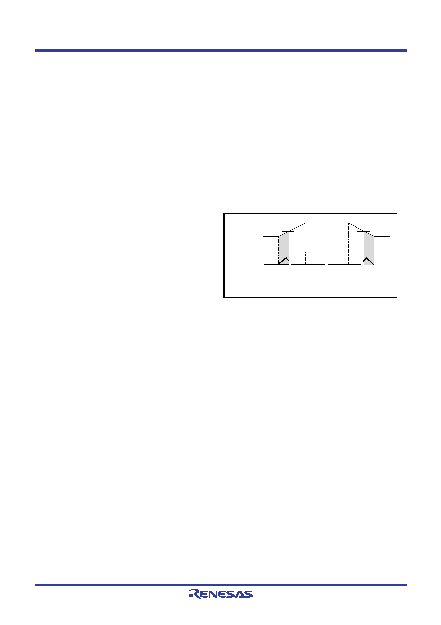
Make sure that voltage exceeding the VCC pin voltage is not
applied to other pins. In particular, ensure that the state indicated
by bold lines in Figure below does not occur for pin CNVSS (VPP
power source pin for QzROM) during power-on or power-off.
Otherwise the contents of QzROM could be rewritten.
Fig 7.
Timing Diagram (bold-lined periods are applicable)
3. QzROM Writing Orders
When ordering the QzROM product shipped after writing,
submit the mask file (extension: .mask) which is made by the
mask file converter MM.
Be sure to set the ROM option (“MASK option” written in the
mask file converter) setup when making the mask file by using
the mask file converter MM.
Be sure to set the ROM option data* setup when making the
mask file by using the mask file converter MM.. The ROM
code protect is specified according to the ROM option data* in
the mask file which is submitted at ordering. Note that the
mask file which has nothing at the ROM option data* or has
the data other than “0016” and “FF16” can not be accepted.
Set “FF16” to the ROM code protect address in ROM data
regardless of the presence or absence of a protect. When data
other than “FF16” is set, we may ask that the ROM data be
submitted again.
* ROM option data: mask option noted in MM
4. Data Required for QzROM Writing Orders
The following are necessary when ordering a QzROM product
shipped after writing:
1. QzROM Writing Confirmation Form*
2. Mark Specification Form*
3. ROM data...........Mask file
* For the QzROM writing confirmation form and the mark
specification form, refer to the “Renesas Technology Corp.”
Homepage (http://www.renesas.com/homepage.jsp).
Note that we cannot deal with special font marking (customer's
trademark etc.) in QzROM microcomputer.
VCC pin voltage
CNVSS pin voltage
“L” input
(1) Input voltage to other MCU pins rises before Vcc pin voltage.
(2) Input voltage to other MCU pins falls after Vcc pin voltage.
Note: The internal circuitry is unstable when Vcc is below the minimum voltage
specification of 1.8 V (shaded portion), so particular care should be
exercised regarding overvoltage.
1.8V
~ ~
相关PDF资料 |
PDF描述 |
|---|---|
| M37545G4KP | 8-BIT, MROM, 4 MHz, MICROCONTROLLER, PDSO32 |
| M37546G4SP | 8-BIT, MROM, 8 MHz, MICROCONTROLLER, PDIP32 |
| M30201F6FP | 16-BIT, FLASH, 10 MHz, MICROCONTROLLER, PQFP56 |
| M30201F6TFP | 16-BIT, FLASH, 10 MHz, MICROCONTROLLER, PQFP56 |
| MB90543GSPMC | 16-BIT, MROM, 16 MHz, MICROCONTROLLER, PQFP100 |
相关代理商/技术参数 |
参数描述 |
|---|---|
| M37545G6GP | 制造商:RENESAS 制造商全称:Renesas Technology Corp 功能描述:SINGLE-CHIP 8-BIT CMOS MICROCOMPUTER |
| M37545G6GP#U0 | 功能描述:MCU 3/5V 24K 32-LQFP QZ-ROM RoHS:是 类别:集成电路 (IC) >> 嵌入式 - 微控制器, 系列:740/38000 标准包装:250 系列:80C 核心处理器:8051 芯体尺寸:8-位 速度:16MHz 连通性:EBI/EMI,I²C,UART/USART 外围设备:POR,PWM,WDT 输入/输出数:40 程序存储器容量:- 程序存储器类型:ROMless EEPROM 大小:- RAM 容量:256 x 8 电压 - 电源 (Vcc/Vdd):4.5 V ~ 5.5 V 数据转换器:A/D 8x10b 振荡器型:内部 工作温度:-40°C ~ 85°C 封装/外壳:68-LCC(J 形引线) 包装:带卷 (TR) |
| M37545G6KP | 制造商:RENESAS 制造商全称:Renesas Technology Corp 功能描述:SINGLE-CHIP 8-BIT CMOS MICROCOMPUTER |
| M37545G6-XXXGP | 制造商:RENESAS 制造商全称:Renesas Technology Corp 功能描述:SINGLE-CHIP 8-BIT CMOS MICROCOMPUTER |
| M37545G8GP | 制造商:RENESAS 制造商全称:Renesas Technology Corp 功能描述:SINGLE-CHIP 8-BIT CMOS MICROCOMPUTER |
发布紧急采购,3分钟左右您将得到回复。