- 您现在的位置:买卖IC网 > PDF目录45045 > M38503E4SP 8-BIT, OTPROM, 4 MHz, MICROCONTROLLER, PDIP42 PDF资料下载
参数资料
| 型号: | M38503E4SP |
| 元件分类: | 微控制器/微处理器 |
| 英文描述: | 8-BIT, OTPROM, 4 MHz, MICROCONTROLLER, PDIP42 |
| 封装: | 0.600 INCH, 1.78 MM PITCH, PLASTIC, SDIP-42 |
| 文件页数: | 257/286页 |
| 文件大小: | 3016K |
| 代理商: | M38503E4SP |
第1页第2页第3页第4页第5页第6页第7页第8页第9页第10页第11页第12页第13页第14页第15页第16页第17页第18页第19页第20页第21页第22页第23页第24页第25页第26页第27页第28页第29页第30页第31页第32页第33页第34页第35页第36页第37页第38页第39页第40页第41页第42页第43页第44页第45页第46页第47页第48页第49页第50页第51页第52页第53页第54页第55页第56页第57页第58页第59页第60页第61页第62页第63页第64页第65页第66页第67页第68页第69页第70页第71页第72页第73页第74页第75页第76页第77页第78页第79页第80页第81页第82页第83页第84页第85页第86页第87页第88页第89页第90页第91页第92页第93页第94页第95页第96页第97页第98页第99页第100页第101页第102页第103页第104页第105页第106页第107页第108页第109页第110页第111页第112页第113页第114页第115页第116页第117页第118页第119页第120页第121页第122页第123页第124页第125页第126页第127页第128页第129页第130页第131页第132页第133页第134页第135页第136页第137页第138页第139页第140页第141页第142页第143页第144页第145页第146页第147页第148页第149页第150页第151页第152页第153页第154页第155页第156页第157页第158页第159页第160页第161页第162页第163页第164页第165页第166页第167页第168页第169页第170页第171页第172页第173页第174页第175页第176页第177页第178页第179页第180页第181页第182页第183页第184页第185页第186页第187页第188页第189页第190页第191页第192页第193页第194页第195页第196页第197页第198页第199页第200页第201页第202页第203页第204页第205页第206页第207页第208页第209页第210页第211页第212页第213页第214页第215页第216页第217页第218页第219页第220页第221页第222页第223页第224页第225页第226页第227页第228页第229页第230页第231页第232页第233页第234页第235页第236页第237页第238页第239页第240页第241页第242页第243页第244页第245页第246页第247页第248页第249页第250页第251页第252页第253页第254页第255页第256页当前第257页第258页第259页第260页第261页第262页第263页第264页第265页第266页第267页第268页第269页第270页第271页第272页第273页第274页第275页第276页第277页第278页第279页第280页第281页第282页第283页第284页第285页第286页
HARDWARE
3850 Group (Spec. H) User’s Manual
FUNCTIONAL DESCRIPTION
1-53
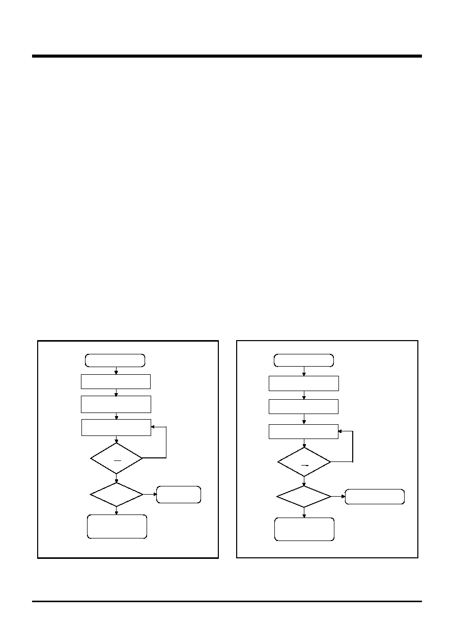
Fig. 54 Block erase flowchart
Program Command (4016)
The program operation starts when the command code “4016” is writ-
ten in the first bus cycle. Then, if the address and data to program
are written in the 2nd bus cycle, program operation (data program-
ming and verification) will start.
Whether the write operation is completed can be confirmed by read-
_____
ing the status register or the RY/BY signal status. When the program
starts, the read status register mode is accessed automatically and
the content of the status register can be read out from the data bus
(D0–D7). The status register bit 7 (SR7) is set to “0” at the same time
the write operation starts and is returned to “1” upon completion of
the write operation. In this case, the read status register mode re-
mains active until the read array command (FF16) is written.
____
The RY/BY pin is “L” during write operation and “H” when the write
operation is completed as is the status register bit 7.
At program end, program results can be checked by reading the sta-
tus register.
Erase All Blocks Command (2016/2016)
By writing the command code “2016” in the first bus cycle and the
confirmation command code “2016” in the second bus cycle that fol-
lows, the system starts erase all blocks( erase and erase verify).
Whether the erase all blocks command is terminated can be con-
____
firmed by reading the status register or the RY/BY signal status .
When the erase all blocks operation starts, the read status register
mode is accessed automatically and the content of the status regis-
ter can be read out. The status register bit 7 (SR7) is set to “0” at the
same time the erase operation starts and is returned to “1” upon
completion of the erase operation. In this case, the read status regis-
ter mode remains active until the read array command (FF16) is writ-
ten.
____
The RY/BY pin is “L” during erase operation and “H” when the erase
operation is completed as is the status register bit 7.
At erase all blocks end, erase results can be checked by reading the
status register. For details, refer to the section where the status reg-
ister is detailed.
Block Erase Command (2016/D016)
By writing the command code “2016” in the first bus cycle and the
confirmation command code “D016” in the second bus cycle that
follows to the block address of a flash memory block, the system
initiates a block erase (erase and erase verify) operation.
Whether the block erase operation is completed can be confirmed
____
by reading the status register or the RY/BY signal. At the same time
the block erase operation starts, the read status register mode is
automatically entered, so the content of the status register can be
read out. The status register bit 7 (SR7) is set to “0” at the same time
the block erase operation starts and is returned to “1” upon comple-
tion of the block erase operation. In this case, the read status regis-
ter mode remains active until the read array command (FF16) is writ-
ten.
____
The RY/BY pin is “L” during block erase operation and “H” when the
block erase operation is completed as is the status register bit 7.
After the block erase operation is completed, the status register can
be read out to know the result of the block erase operation. For de-
tails, refer to the section where the status register is detailed.
Fig. 53 Page program flowchart
Start
Write 4016
Status register
read
Program completed
(Read command
FF16 write)
NO
YES
Write address
Write data
SR4=0?
Program
error
NO
YES
SR7=1?
or
RY/BY=1?
Write
Write 2016
2016/D016
Block address
Erase completed
(Read command
FF16 write)
NO
YES
Start
Write
SR5=0?
Erase error
YES
NO
2016:Erase all blocks
D016:Block erase
SR7=1?
or
RY/BY=1?
Status register
read
相关PDF资料 |
PDF描述 |
|---|---|
| M38503E4FP | 8-BIT, OTPROM, 4 MHz, MICROCONTROLLER, PDSO42 |
| M38503M6-XXXFP | 8-BIT, MROM, 8 MHz, MICROCONTROLLER, PDSO42 |
| M38503E6SP | 8-BIT, OTPROM, 8 MHz, MICROCONTROLLER, PDIP42 |
| M38504E6FP | 8-BIT, MROM, 8 MHz, MICROCONTROLLER, PDSO42 |
| M38504M6-XXXSP | 8-BIT, MROM, 8 MHz, MICROCONTROLLER, PDIP42 |
相关代理商/技术参数 |
参数描述 |
|---|---|
| M38503G4AFP#U1 | 功能描述:IC 740/3850 MCU QZ-ROM 42SSOP RoHS:是 类别:集成电路 (IC) >> 嵌入式 - 微控制器, 系列:740/38000 标准包装:250 系列:80C 核心处理器:8051 芯体尺寸:8-位 速度:16MHz 连通性:EBI/EMI,I²C,UART/USART 外围设备:POR,PWM,WDT 输入/输出数:40 程序存储器容量:- 程序存储器类型:ROMless EEPROM 大小:- RAM 容量:256 x 8 电压 - 电源 (Vcc/Vdd):4.5 V ~ 5.5 V 数据转换器:A/D 8x10b 振荡器型:内部 工作温度:-40°C ~ 85°C 封装/外壳:68-LCC(J 形引线) 包装:带卷 (TR) |
| M38503G4ASP#U1 | 功能描述:IC 740/3850 MCU QZ-ROM 42DIP RoHS:是 类别:集成电路 (IC) >> 嵌入式 - 微控制器, 系列:740/38000 标准包装:250 系列:80C 核心处理器:8051 芯体尺寸:8-位 速度:16MHz 连通性:EBI/EMI,I²C,UART/USART 外围设备:POR,PWM,WDT 输入/输出数:40 程序存储器容量:- 程序存储器类型:ROMless EEPROM 大小:- RAM 容量:256 x 8 电压 - 电源 (Vcc/Vdd):4.5 V ~ 5.5 V 数据转换器:A/D 8x10b 振荡器型:内部 工作温度:-40°C ~ 85°C 封装/外壳:68-LCC(J 形引线) 包装:带卷 (TR) |
| M38503M2404F | 制造商:Panasonic Industrial Company 功能描述:IC |
| M38503M4A-210SP | 制造商:Renesas Electronics Corporation 功能描述: |
| M38504E6FP | 制造商:Renesas Electronics Corporation 功能描述:MCU 3/5V 24K 42-SSOP - Trays |
发布紧急采购,3分钟左右您将得到回复。