- 您现在的位置:买卖IC网 > PDF目录383302 > M50FW040K5TG (意法半导体) 4-Mbit (512 Kb x8, uniform block) 3-V supply firmware hub Flash memory PDF资料下载
参数资料
| 型号: | M50FW040K5TG |
| 厂商: | 意法半导体 |
| 英文描述: | 4-Mbit (512 Kb x8, uniform block) 3-V supply firmware hub Flash memory |
| 中文描述: | 4兆位(512 KB的× 8,均匀块)3 - V电源供电的闪存固件枢纽 |
| 文件页数: | 20/53页 |
| 文件大小: | 278K |
| 代理商: | M50FW040K5TG |
第1页第2页第3页第4页第5页第6页第7页第8页第9页第10页第11页第12页第13页第14页第15页第16页第17页第18页第19页当前第20页第21页第22页第23页第24页第25页第26页第27页第28页第29页第30页第31页第32页第33页第34页第35页第36页第37页第38页第39页第40页第41页第42页第43页第44页第45页第46页第47页第48页第49页第50页第51页第52页第53页
Bus operations
M50FW040
20/53
Table 4.
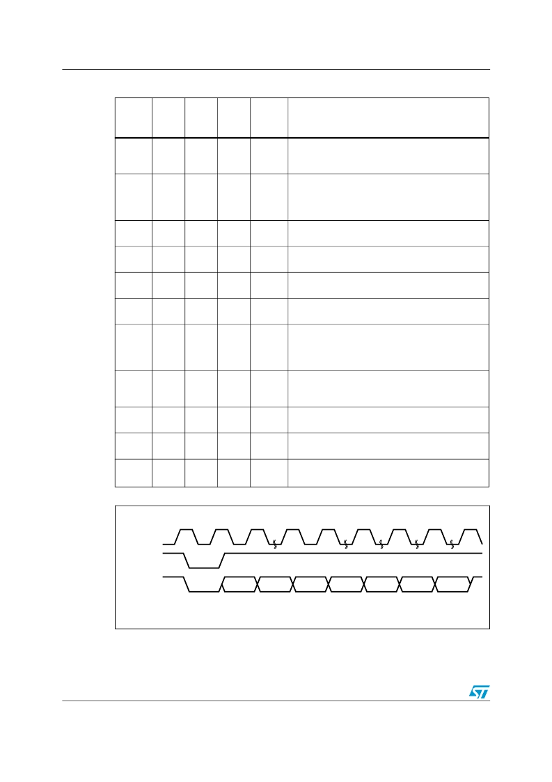
Figure 6.
FWH Bus Read waveforms
FWH bus Read field definitions
Clock
Cycle
Number
Clock
Cycle
Count
Field
FWH0-
FWH3
Memory
I/O
Description
1
1
START
1101b
I
On the rising edge of CLK with FWH4 Low, the
contents of FWH0-FWH3 indicate the start of a FWH
Read cycle.
2
1
IDSEL
XXXX
I
Indicates which FWH Flash Memory is selected. The
value on FWH0-FWH3 is compared to the IDSEL
strapping on the FWH Flash Memory pins to select
which FWH Flash Memory is being addressed.
3-9
7
ADDR
XXXX
I
A 28-bit address phase is transferred starting with
the most significant nibble first.
10
1
MSIZE
0000b
I
Always 0000b (only single byte transfers are
supported).
11
1
TAR
1111b
I
The host drives FWH0-FWH3 to 1111b to indicate a
turnaround cycle.
12
1
TAR
1111b
(float)
O
The FWH Flash Memory takes control of FWH0-
FWH3 during this cycle.
13-14
2
WSYN
C
0101b
O
The FWH Flash Memory drives FWH0-FWH3 to
0101b (short wait-sync) for two clock cycles,
indicating that the data is not yet available. Two wait-
states are always included.
15
1
RSYN
C
0000b
O
The FWH Flash Memory drives FWH0-FWH3 to
0000b, indicating that data will be available during
the next clock cycle.
16-17
2
DATA
XXXX
O
Data transfer is two CLK cycles, starting with the
least significant nibble.
18
1
TAR
1111b
O
The FWH Flash Memory drives FWH0-FWH3 to
1111b to indicate a turnaround cycle.
19
1
TAR
1111b
(float)
N/A
The FWH Flash Memory floats its outputs, the host
takes control of FWH0-FWH3.
AI03437
CLK
FWH4
FWH0-FWH3
Number of
clock cycles
START
IDSEL
ADDR
MSIZE
TAR
SYNC
DATA
TAR
1
1
7
1
2
3
2
2
相关PDF资料 |
PDF描述 |
|---|---|
| M50FW040K5TP | 4-Mbit (512 Kb x8, uniform block) 3-V supply firmware hub Flash memory |
| M50FW040N5G | 4-Mbit (512 Kb x8, uniform block) 3-V supply firmware hub Flash memory |
| M50FW040N5P | 4-Mbit (512 Kb x8, uniform block) 3-V supply firmware hub Flash memory |
| M50FW040N5TG | 4-Mbit (512 Kb x8, uniform block) 3-V supply firmware hub Flash memory |
| M50FW040N5TP | 4-Mbit (512 Kb x8, uniform block) 3-V supply firmware hub Flash memory |
相关代理商/技术参数 |
参数描述 |
|---|---|
| M50FW040K5TP | 制造商:STMICROELECTRONICS 制造商全称:STMicroelectronics 功能描述:4-Mbit (512 Kb x8, uniform block) 3-V supply firmware hub Flash memory |
| M50FW040N | 制造商:STMICROELECTRONICS 制造商全称:STMicroelectronics 功能描述:4 Mbit 512Kb x8, Uniform Block 3V Supply Firmware Hub Flash Memory |
| M50FW040N1 | 功能描述:闪存 3.6V 4M (512Kx8) RoHS:否 制造商:ON Semiconductor 数据总线宽度:1 bit 存储类型:Flash 存储容量:2 MB 结构:256 K x 8 定时类型: 接口类型:SPI 访问时间: 电源电压-最大:3.6 V 电源电压-最小:2.3 V 最大工作电流:15 mA 工作温度:- 40 C to + 85 C 安装风格:SMD/SMT 封装 / 箱体: 封装:Reel |
| M50FW040N1T | 功能描述:闪存 3.6V 4M (512Kx8) RoHS:否 制造商:ON Semiconductor 数据总线宽度:1 bit 存储类型:Flash 存储容量:2 MB 结构:256 K x 8 定时类型: 接口类型:SPI 访问时间: 电源电压-最大:3.6 V 电源电压-最小:2.3 V 最大工作电流:15 mA 工作温度:- 40 C to + 85 C 安装风格:SMD/SMT 封装 / 箱体: 封装:Reel |
| M50FW040N5 | 功能描述:闪存 3.0-3.6V 4M (512Kx8) RoHS:否 制造商:ON Semiconductor 数据总线宽度:1 bit 存储类型:Flash 存储容量:2 MB 结构:256 K x 8 定时类型: 接口类型:SPI 访问时间: 电源电压-最大:3.6 V 电源电压-最小:2.3 V 最大工作电流:15 mA 工作温度:- 40 C to + 85 C 安装风格:SMD/SMT 封装 / 箱体: 封装:Reel |
发布紧急采购,3分钟左右您将得到回复。