- 您现在的位置:买卖IC网 > PDF目录224185 > M95256-RDW6TG (STMICROELECTRONICS) 32K X 8 SPI BUS SERIAL EEPROM, PDSO8 PDF资料下载
参数资料
| 型号: | M95256-RDW6TG |
| 厂商: | STMICROELECTRONICS |
| 元件分类: | PROM |
| 英文描述: | 32K X 8 SPI BUS SERIAL EEPROM, PDSO8 |
| 封装: | 0.169 INCH, ROHS COMPLIANT, TSSOP-8 |
| 文件页数: | 15/44页 |
| 文件大小: | 386K |
| 代理商: | M95256-RDW6TG |
第1页第2页第3页第4页第5页第6页第7页第8页第9页第10页第11页第12页第13页第14页当前第15页第16页第17页第18页第19页第20页第21页第22页第23页第24页第25页第26页第27页第28页第29页第30页第31页第32页第33页第34页第35页第36页第37页第38页第39页第40页第41页第42页第43页第44页
Instructions
M95256, M95256-W, M95256-R
5.6
Write to Memory Array (WRITE)
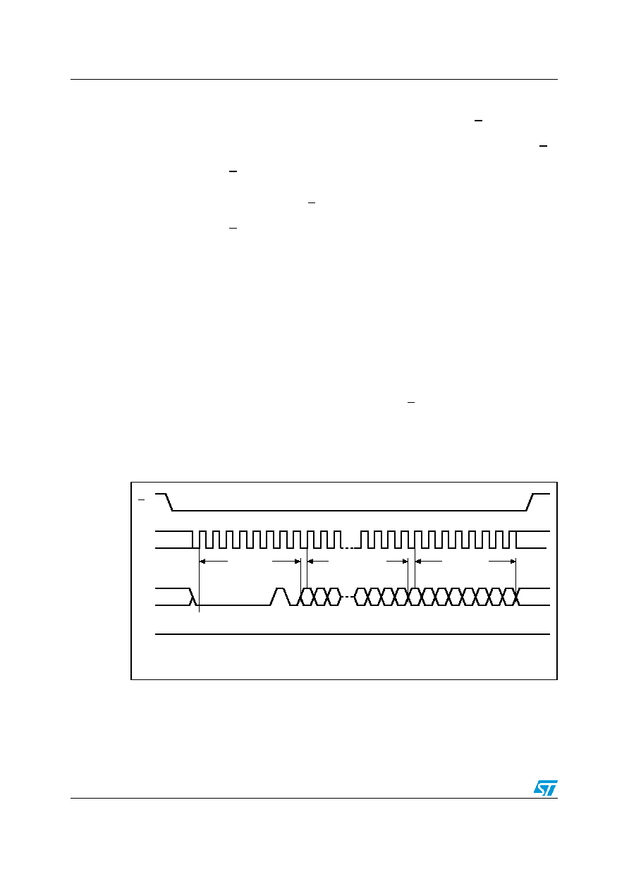
As shown in Figure 11, to send this instruction to the device, Chip Select (S) is first driven
low. The bits of the instruction byte, address bytes, and at least one data byte are then
shifted in, on Serial Data input (D). The instruction is terminated by driving Chip Select (S)
high at a byte boundary of the input data. The self-timed Write cycle, triggered by the rising
Table 18 and Table 19.), at the end of which the Write in Progress (WIP) bit is reset to 0.
In the case of Figure 11, Chip Select (S) is driven high after the eighth bit of the data byte
has been latched in, indicating that the instruction is being used to write a single byte. If,
though, Chip Select (S) continues to be driven low, as shown in Figure 12, the next byte of
input data is shifted in, so that more than a single byte, starting from the given address
towards the end of the same page, can be written in a single internal Write cycle.
Each time a new data byte is shifted in, the least significant bits of the internal address
counter are incremented. If the number of data bytes sent to the device exceeds the page
boundary, the internal address counter rolls over to the beginning of the page, and the
previous data there are overwritten with the incoming data. (The page size of these devices
is 64 bytes).
The instruction is not accepted, and is not executed, under the following conditions:
●
if the Write Enable Latch (WEL) bit has not been set to 1 (by executing a Write Enable
instruction just before)
●
if a Write cycle is already in progress
●
if the device has not been deselected, by Chip Select (S) being driven high, at a byte
boundary (after the eighth bit, b0, of the last data byte that has been latched in)
●
if the addressed page is in the region protected by the Block Protect (BP1 and BP0)
bits.
Figure 11.
Byte Write (WRITE) sequence
1.
The most significant address bit (b15) is Don’t Care.
C
D
AI01795D
S
Q
15
2
1
3456789 10
20 21 22 23 24 25 26 27
14 13
3210
28 29 30
High Impedance
Instruction
16-Bit Address
0
765432
0
1
Data Byte
31
相关PDF资料 |
PDF描述 |
|---|---|
| MA-306-29.4912M-K0 | QUARTZ CRYSTAL RESONATOR, 29.4912 MHz |
| MA04206 | 2-PORT SAW RESONATOR, 433.92 MHz |
| MA05199 | 1-PORT SAW RESONATOR, 434.42 MHz |
| MA1050 | 1 A SWITCHING REGULATOR, 200 kHz SWITCHING FREQ-MAX, SIP7 |
| MA21D35 | 1 A, 30 V, SILICON, SIGNAL DIODE |
相关代理商/技术参数 |
参数描述 |
|---|---|
| M95256-RDW6TG/A | 制造商:STMICROELECTRONICS 制造商全称:STMicroelectronics 功能描述:256 Kbit Serial SPI bus EEPROM with high speed clock |
| M95256-RDW6TG/K | 制造商:STMICROELECTRONICS 制造商全称:STMicroelectronics 功能描述:256 Kbit serial SPI bus EEPROM with high-speed clock |
| M95256-RDW6TG/V | 制造商:STMICROELECTRONICS 制造商全称:STMicroelectronics 功能描述:256 Kbit Serial SPI bus EEPROM with high speed clock |
| M95256RDW6TP | 制造商:STMICROELECTRONICS 制造商全称:STMicroelectronics 功能描述:256 Kbit serial SPI bus EEPROM with high-speed clock |
| M95256-RDW6TP | 功能描述:电可擦除可编程只读存储器 256 Kbit Serial Bus 电可擦除可编程只读存储器 RoHS:否 制造商:Atmel 存储容量:2 Kbit 组织:256 B x 8 数据保留:100 yr 最大时钟频率:1000 KHz 最大工作电流:6 uA 工作电源电压:1.7 V to 5.5 V 最大工作温度:+ 85 C 安装风格:SMD/SMT 封装 / 箱体:SOIC-8 |
发布紧急采购,3分钟左右您将得到回复。