- 您现在的位置:买卖IC网 > PDF目录224185 > M95256-RDW6TG (STMICROELECTRONICS) 32K X 8 SPI BUS SERIAL EEPROM, PDSO8 PDF资料下载
参数资料
| 型号: | M95256-RDW6TG |
| 厂商: | STMICROELECTRONICS |
| 元件分类: | PROM |
| 英文描述: | 32K X 8 SPI BUS SERIAL EEPROM, PDSO8 |
| 封装: | 0.169 INCH, ROHS COMPLIANT, TSSOP-8 |
| 文件页数: | 5/44页 |
| 文件大小: | 386K |
| 代理商: | M95256-RDW6TG |
第1页第2页第3页第4页当前第5页第6页第7页第8页第9页第10页第11页第12页第13页第14页第15页第16页第17页第18页第19页第20页第21页第22页第23页第24页第25页第26页第27页第28页第29页第30页第31页第32页第33页第34页第35页第36页第37页第38页第39页第40页第41页第42页第43页第44页
M95256, M95256-W, M95256-R
Operating features
4.2
Status Register
Figure 4 shows the position of the Status Register in the control logic of the device. The
Status Register contains a number of status and control bits that can be read or set (as
appropriate) by specific instructions. For a detailed description of the Status Register bits,
4.3
Data protection and protocol control
Non-volatile memory devices can be used in environments that are particularly noisy, and
within applications that could experience problems if memory bytes are corrupted.
Consequently, the device features the following data protection mechanisms:
●
Write and Write Status Register instructions are checked that they consist of a number
of clock pulses that is a multiple of eight, before they are accepted for execution.
●
All instructions that modify data must be preceded by a Write Enable (WREN)
instruction to set the Write Enable Latch (WEL) bit. This bit is returned to its reset state
by the following events:
–Power-up
–
Write Disable (WRDI) instruction completion
–
Write Status Register (WRSR) instruction completion
–
Write (WRITE) instruction completion
●
The Block Protect (BP1, BP0) bits in the Status Register allow part of the memory to be
configured as read-only.
●
The Write Protect (W) signal allows the Block Protect (BP1, BP0) bits of the Status
Register to be protected.
For any instruction to be accepted, and executed, Chip Select (S) must be driven high after
the rising edge of Serial Clock (C) for the last bit of the instruction, and before the next rising
edge of Serial Clock (C).
Two points need to be noted in the previous sentence:
●
The ‘last bit of the instruction’ can be the eighth bit of the instruction code, or the eighth
bit of a data byte, depending on the instruction (except for Read Status Register
(RDSR) and Read (READ) instructions).
●
The ‘next rising edge of Serial Clock (C)’ might (or might not) be the next bus
transaction for some other device on the SPI bus.
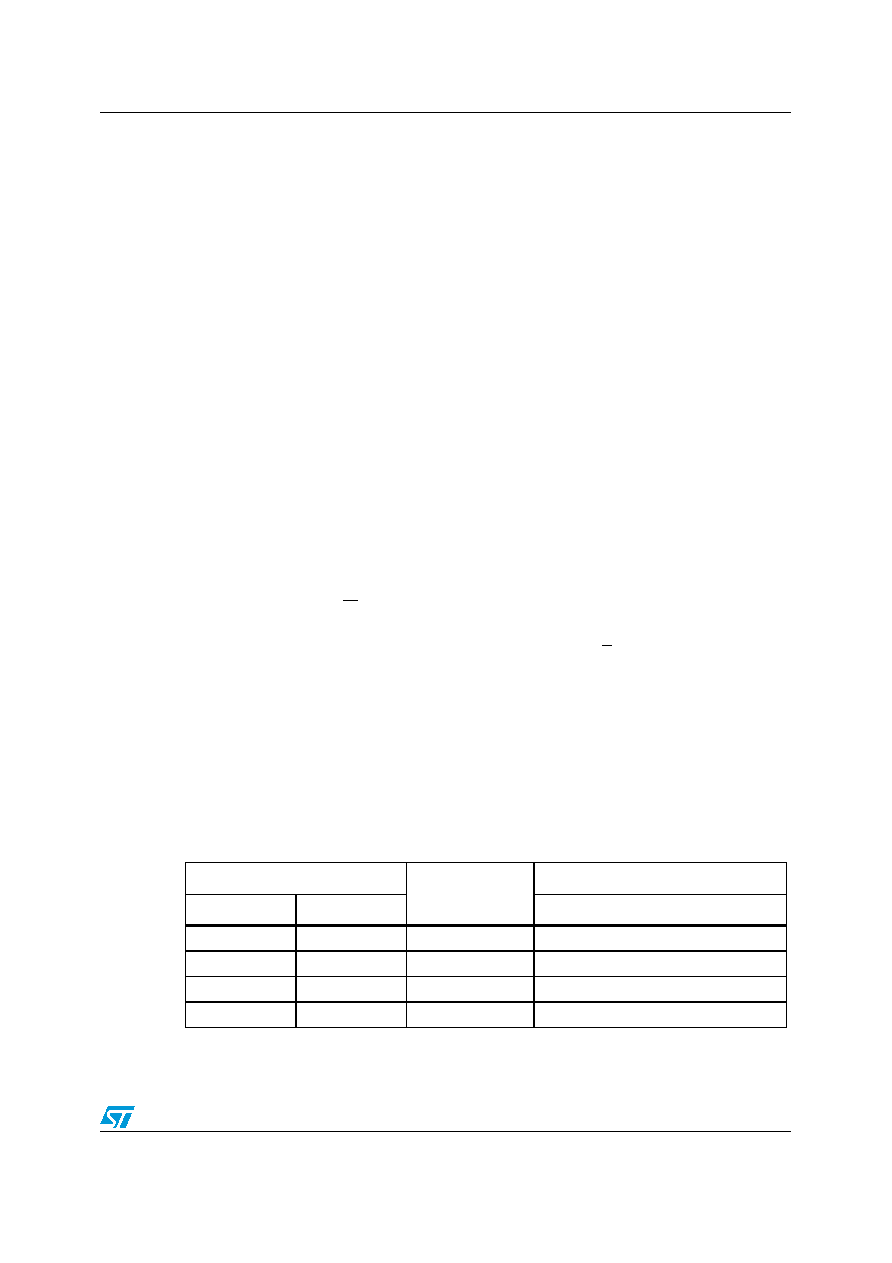
Table 2.
Write-protected block size
Status Register bits
Protected block
Protected array addresse
BP1
BP0
M95256, M95256-W, M95256-R
0
none
0
1
Upper quarter
6000h - 7FFFh
1
0
Upper half
4000h - 7FFFh
1
Whole memory
0000h - 7FFFh
相关PDF资料 |
PDF描述 |
|---|---|
| MA-306-29.4912M-K0 | QUARTZ CRYSTAL RESONATOR, 29.4912 MHz |
| MA04206 | 2-PORT SAW RESONATOR, 433.92 MHz |
| MA05199 | 1-PORT SAW RESONATOR, 434.42 MHz |
| MA1050 | 1 A SWITCHING REGULATOR, 200 kHz SWITCHING FREQ-MAX, SIP7 |
| MA21D35 | 1 A, 30 V, SILICON, SIGNAL DIODE |
相关代理商/技术参数 |
参数描述 |
|---|---|
| M95256-RDW6TG/A | 制造商:STMICROELECTRONICS 制造商全称:STMicroelectronics 功能描述:256 Kbit Serial SPI bus EEPROM with high speed clock |
| M95256-RDW6TG/K | 制造商:STMICROELECTRONICS 制造商全称:STMicroelectronics 功能描述:256 Kbit serial SPI bus EEPROM with high-speed clock |
| M95256-RDW6TG/V | 制造商:STMICROELECTRONICS 制造商全称:STMicroelectronics 功能描述:256 Kbit Serial SPI bus EEPROM with high speed clock |
| M95256RDW6TP | 制造商:STMICROELECTRONICS 制造商全称:STMicroelectronics 功能描述:256 Kbit serial SPI bus EEPROM with high-speed clock |
| M95256-RDW6TP | 功能描述:电可擦除可编程只读存储器 256 Kbit Serial Bus 电可擦除可编程只读存储器 RoHS:否 制造商:Atmel 存储容量:2 Kbit 组织:256 B x 8 数据保留:100 yr 最大时钟频率:1000 KHz 最大工作电流:6 uA 工作电源电压:1.7 V to 5.5 V 最大工作温度:+ 85 C 安装风格:SMD/SMT 封装 / 箱体:SOIC-8 |
发布紧急采购,3分钟左右您将得到回复。