- 您现在的位置:买卖IC网 > PDF目录17007 > MAX1132EVKIT (Maxim Integrated Products)KIT EVAL FOR MAX1132 PDF资料下载
参数资料
| 型号: | MAX1132EVKIT |
| 厂商: | Maxim Integrated Products |
| 文件页数: | 12/19页 |
| 文件大小: | 0K |
| 描述: | KIT EVAL FOR MAX1132 |
| 产品培训模块: | Lead (SnPb) Finish for COTS Obsolescence Mitigation Program |
| 标准包装: | 1 |
| ADC 的数量: | 1 |
| 位数: | 16 |
| 采样率(每秒): | 200k |
| 数据接口: | 串行 |
| 输入范围: | ±12 V |
| 在以下条件下的电源(标准): | 55mW @ 200kSPS |
| 工作温度: | 0°C ~ 70°C |
| 已用 IC / 零件: | MAX1132,MAX1133 |
| 已供物品: | 板,CD |
MAX1132/MAX1133
16-Bit ADC, 200ksps, 5V Single-Supply
with Reference
2
_______________________________________________________________________________________
ABSOLUTE MAXIMUM RATINGS
Stresses beyond those listed under “Absolute Maximum Ratings” may cause permanent damage to the device. These are stress ratings only, and functional
operation of the device at these or any other conditions beyond those indicated in the operational sections of the specifications is not implied. Exposure to
absolute maximum rating conditions for extended periods may affect device reliability.
AVDD to AGND, DVDD to DGND .............................-0.3V to +6V
AGND to DGND.....................................................-0.3V to +0.3V
AIN to AGND.....................................................................±16.5V
REFADJ, CREF, REF to AGND.................-0.3V to (AVDD + 0.3V)
Digital Inputs to DGND.............................................-0.3V to +6V
Digital Outputs to DGND .........................-0.3V to (DVDD + 0.3V)
Continuous Power Dissipation (TA = +70°C)
20-Pin SSOP (derate 8.00mW/°C above +70°C) .........640mW
Operating Temperature Ranges
MAX113_CAP ......................................................0°C to +70°C
MAX113_EAP....................................................-40°C to +85°C
Storage Temperature Range .............................-60°C to +150°C
Junction Temperature ......................................................+150°C
Lead Temperature (soldering, 10s) .................................+300°C
ELECTRICAL CHARACTERISTICS
(AVDD = DVDD = +5V ±5%, fSCLK = 4.8MHz, external clock (50% duty cycle), 24 clocks/conversion (200ksps), bipolar input, external
VREF = +4.096V, VREFADJ = AVDD, CREF = 2.2F, CCREF = 1F, TA = TMIN to TMAX, unless otherwise noted. Typical values are at
TA = +25°C.)
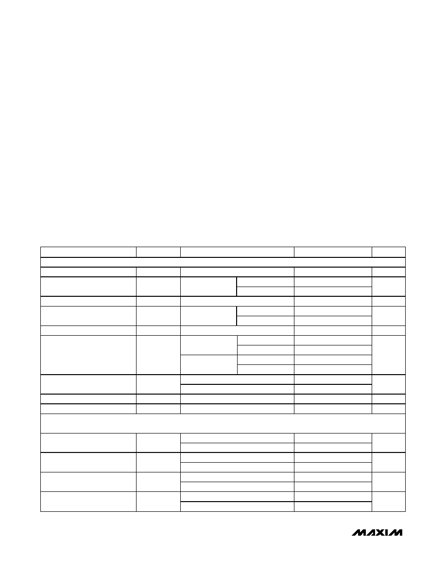
PARAMETER
SYMBOL
CONDITIONS
MIN
TYP
MAX
UNITS
DC ACCURACY (Note 1)
Resolution
16
Bits
MAX113_A
±1.5
Relative Accuracy (Note 2)
INL
Bipolar mode
MAX113_B
±2.5
LSB
No Missing Codes
16
Bits
MAX113_A
-1
+1
Differential Nonlinearity
DNL
Bipolar mode
MAX113_B
-1
+1.75
LSB
Transition Noise
0.77
LSBRMS
MAX1132
±4
Unipolar
MAX1133
±2
MAX1132
±6
Offset Error
Bipolar
MAX1133
±5
mV
Unipolar
±0.2
Gain Error (Note 3)
Bipolar
±0.3
%FSR
Offset Drift (Bipolar and Unipolar)
Excluding reference drift
±1
ppm/
oC
Gain Drift (Bipolar and Unipolar)
Excluding reference drift
±1
ppm/
oC
DYNAMIC SPECIFICATIONS (5kHz sine-wave input, 200ksps, 4.8MHz clock, bipolar input mode. MAX1132: 24Vp-p.
MAX1133: 8.192Vp-p)
fIN = 5kHz
85
SINAD
fIN = 100kHz
85
dB
fIN = 5kHz
87
SNR
fIN = 100kHz
92
dB
fIN = 5kHz
-90
THD
fIN = 100kHz
-92
dB
fIN = 5kHz
92
SFDR
fIN = 100kHz
96
dB
相关PDF资料 |
PDF描述 |
|---|---|
| HCM10DRTI-S13 | CONN EDGECARD 20POS .156 EXTEND |
| AC2626K4 | PROBE TEMP 4" GENERAL PURP |
| HBM10DRTI-S13 | CONN EDGECARD 20POS .156 EXTEND |
| 0210490252 | CABLE JUMPER 1.25MM .254M 18POS |
| ADZS-AUDIO-EX3 | BOARD EXTENDER AUDIO EI3 |
相关代理商/技术参数 |
参数描述 |
|---|---|
| MAX1132EVSYS | 制造商:MAXIM 制造商全称:Maxim Integrated Products 功能描述:Evaluation System for the MAX1132/MAX1133 |
| MAX1132-MAX1133 | 制造商:MAXIM 制造商全称:Maxim Integrated Products 功能描述:16-Bit ADC, 200ksps, 5V Single-Supply with Reference |
| MAX1133 | 制造商:MAXIM 制造商全称:Maxim Integrated Products 功能描述:16-Bit ADC, 200ksps, 5V Single-Supply with Reference |
| MAX11330 | 制造商:MAXIM 制造商全称:Maxim Integrated Products 功能描述:3Msps, 12-/10-Bit, 8-/16-Channel ADCs with Post-Mux External Signal Conditioning Access |
| MAX11330ATJ | 制造商:MAXIM 制造商全称:Maxim Integrated Products 功能描述:3Msps, 12-/10-Bit, 8-/16-Channel ADCs with Post-Mux External Signal Conditioning Access |
发布紧急采购,3分钟左右您将得到回复。