- 您现在的位置:买卖IC网 > PDF目录17007 > MAX1132EVKIT (Maxim Integrated Products)KIT EVAL FOR MAX1132 PDF资料下载
参数资料
| 型号: | MAX1132EVKIT |
| 厂商: | Maxim Integrated Products |
| 文件页数: | 5/19页 |
| 文件大小: | 0K |
| 描述: | KIT EVAL FOR MAX1132 |
| 产品培训模块: | Lead (SnPb) Finish for COTS Obsolescence Mitigation Program |
| 标准包装: | 1 |
| ADC 的数量: | 1 |
| 位数: | 16 |
| 采样率(每秒): | 200k |
| 数据接口: | 串行 |
| 输入范围: | ±12 V |
| 在以下条件下的电源(标准): | 55mW @ 200kSPS |
| 工作温度: | 0°C ~ 70°C |
| 已用 IC / 零件: | MAX1132,MAX1133 |
| 已供物品: | 板,CD |
the beginning of calibration and goes high to signal the
end of calibration, approximately 80,000 clock cycles
later. In external clock mode, SSTRB goes high at the
beginning of calibration and goes low to signal the end
of calibration. Calibration should be performed in the
same clock mode as will be used for conversions.
Reference
The MAX1132/MAX1133 can be used with an internal
or external reference. An external reference can be
connected directly at the REF pin or at the REFADJ pin.
CREF is an internal reference node and must be
bypassed with a 1F capacitor when using either the
internal or an external reference.
Internal Reference
When using the MAX1132/MAX1133’s internal refer-
ence, place a 0.22F ceramic capacitor from REFADJ
to AGND and place a 2.2F capacitor from REF to
AGND. Fine adjustments can be made to the internal
reference voltage by sinking or sourcing current at
REFADJ. The input impedance of REFADJ is nominally
9k. The internal reference voltage is adjustable to
±1.5% with the circuit of Figure 7.
External reference
An external reference can be placed at either the input
(REFADJ) or the output (REF) of the MAX1132/
MAX1133’s internal buffer amplifier.
When connecting an external reference to REFADJ, the
input impedance is typically 9k. Using the buffered
REFADJ input makes buffering of the external reference
unnecessary, however, the internal buffer output must
be bypassed at REF with a 2.2F capacitor.
When connecting an external reference at REF,
REFADJ must be connected to AVDD. Then the input
impedance at REF is a minimum of 164k for DC cur-
rents. During conversion, an external reference at REF
must deliver 250A DC load current and have an out-
put impedance of 10 or less. If the reference has a
higher output impedance or is noisy, bypass it at the
REF pin with a 4.7F capacitor.
Analog Input
The MAX1132/MAX1133 use a capacitive DAC that
provides an inherent track/hold function. Drive AIN with
a source impedance less than 10. Any signal condi-
tioning circuitry must settle with 16-bit accuracy in less
than 500ns. Limit the input bandwidth to less than half
the sampling frequency to eliminate aliasing. The
MAX1132/MAX1133 has a complex input impedance
which varies from unipolar to bipolar mode (Figure 1).
Input Range
The analog input range in unipolar mode is 0 to +12V
for the MAX1132, and 0 to +4.096V for the MAX1133. In
bipolar mode, the analog input can be -12V to +12V for
the MAX1132, and -4.096V to +4.096V for the
MAX1133. Unipolar and bipolar mode is programmed
with the UNI/
BIP bit of the Control Byte. When using a
reference other than the MAX1132/MAX1133’s internal
+4.096V reference, the full-scale input range will vary
accordingly. The full-scale input range depends on the
voltage at REF and the sampling mode selected (Tables
3 and 4).
Input Acquisition and Settling
Clocking in a Control Byte starts input acquisition. In
bipolar mode the main capacitor array starts acquiring
the input as soon as a start bit is recognized. If unipolar
mode is selected by the second DIN bit, the part will
immediately switch to unipolar sampling mode and
acquire a sample.
Acquisition can be extended by eight clock cycles by
setting M1 = 1, M0 = 1 (long acquisition mode). The
sampling instant in short acquisition completes on the
falling edge of the sixth clock cycle after the start bit
(Figure 2).
Acquisition is 5.5 clock cycles in short acquisition
mode and 13.5 clock cycles in long acquisition mode.
Short acquisition mode is 24 clock cycles per conver-
sion. Using the external clock to run the conversion
process limits unipolar conversion speed to 125ksps
instead of 200ksps in bipolar mode. The input resis-
tance in unipolar mode is larger than that of bipolar
mode (Figure1). The RC time constant in unipolar mode
is larger than that of bipolar mode, reducing the maxi-
mum conversion rate in 24 external clock mode. Long
acquisition mode with external clock allows both unipo-
lar and bipolar sampling of 150ksps (4.8MHz/32 clock
cycles) by adding eight extra clock cycles to the con-
version.
MAX1132/MAX1133
16-Bit ADC, 200ksps, 5V Single-Supply
with Reference
______________________________________________________________________________________
13
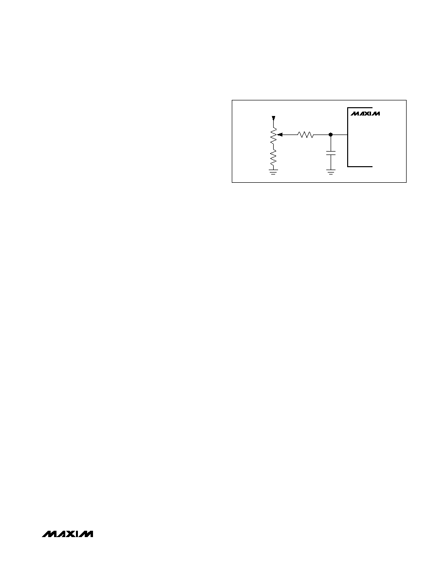
+5V
510k
100k
24k
0.22F
REFADJ
MAX1132
Figure 7. MAX1132 Reference-Adjust Circuit
相关PDF资料 |
PDF描述 |
|---|---|
| HCM10DRTI-S13 | CONN EDGECARD 20POS .156 EXTEND |
| AC2626K4 | PROBE TEMP 4" GENERAL PURP |
| HBM10DRTI-S13 | CONN EDGECARD 20POS .156 EXTEND |
| 0210490252 | CABLE JUMPER 1.25MM .254M 18POS |
| ADZS-AUDIO-EX3 | BOARD EXTENDER AUDIO EI3 |
相关代理商/技术参数 |
参数描述 |
|---|---|
| MAX1132EVSYS | 制造商:MAXIM 制造商全称:Maxim Integrated Products 功能描述:Evaluation System for the MAX1132/MAX1133 |
| MAX1132-MAX1133 | 制造商:MAXIM 制造商全称:Maxim Integrated Products 功能描述:16-Bit ADC, 200ksps, 5V Single-Supply with Reference |
| MAX1133 | 制造商:MAXIM 制造商全称:Maxim Integrated Products 功能描述:16-Bit ADC, 200ksps, 5V Single-Supply with Reference |
| MAX11330 | 制造商:MAXIM 制造商全称:Maxim Integrated Products 功能描述:3Msps, 12-/10-Bit, 8-/16-Channel ADCs with Post-Mux External Signal Conditioning Access |
| MAX11330ATJ | 制造商:MAXIM 制造商全称:Maxim Integrated Products 功能描述:3Msps, 12-/10-Bit, 8-/16-Channel ADCs with Post-Mux External Signal Conditioning Access |
发布紧急采购,3分钟左右您将得到回复。