- 您现在的位置:买卖IC网 > PDF目录17007 > MAX1132EVKIT (Maxim Integrated Products)KIT EVAL FOR MAX1132 PDF资料下载
参数资料
| 型号: | MAX1132EVKIT |
| 厂商: | Maxim Integrated Products |
| 文件页数: | 17/19页 |
| 文件大小: | 0K |
| 描述: | KIT EVAL FOR MAX1132 |
| 产品培训模块: | Lead (SnPb) Finish for COTS Obsolescence Mitigation Program |
| 标准包装: | 1 |
| ADC 的数量: | 1 |
| 位数: | 16 |
| 采样率(每秒): | 200k |
| 数据接口: | 串行 |
| 输入范围: | ±12 V |
| 在以下条件下的电源(标准): | 55mW @ 200kSPS |
| 工作温度: | 0°C ~ 70°C |
| 已用 IC / 零件: | MAX1132,MAX1133 |
| 已供物品: | 板,CD |
MAX1132/MAX1133
16-Bit ADC, 200ksps, 5V Single-Supply
with Reference
_______________________________________________________________________________________
7
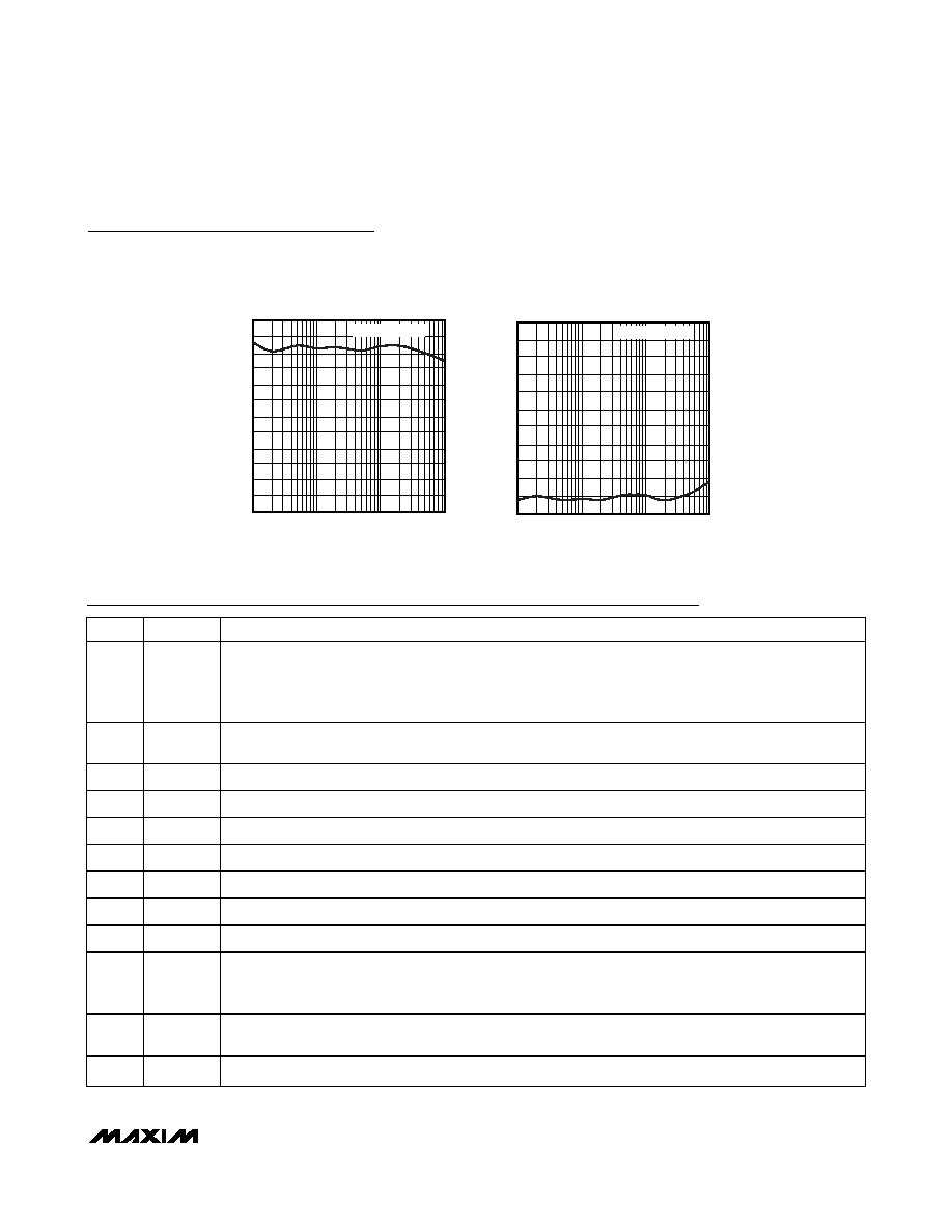
Typical Operating Characteristics (continued)
(MAX1132/MAX1133: AVDD = DVDD = +5V , fSCLK = 4.8MHz, external clock (50% duty cycle), 24 clocks/conversion (200ksps),
bipolar input, external REF = +4.096V, 0.22F bypassing on REFADJ, 2.2F on REF, 1F on CREF, TA = 25°C, unless otherwise noted.)
0
0.1
100
10
1
SFDR PLOT
120
MAX1132
toc10
FREQUENCY (kHz)
AMPLITUDE
(dB)
100
80
60
40
10
20
30
110
90
70
50
fSAMPLE = 200kHz
-110
0.1
100
10
1
THD PLOT
0
MAX1132
toc11
FREQUENCY (kHz)
AMPLITUDE
(dB)
-10
-30
-50
-70
-100
-90
-80
-20
-40
-60
fSAMPLE = 200kHz
PIN
NAME
FUNCTION
1
REF
Reference Buffer Output/ADC Reference Input. Reference voltage for analog-to-digital conversion. In
internal reference mode, the reference buffer provides a +4.096V nominal output, externally adjustable at
REFADJ. In external reference mode, disable the internal buffer by pulling REFADJ to AVDD. Bypass to
AGND with a 2.2F capacitor when using the internal reference.
2
REFADJ
Bandgap Reference Output/Bandgap Reference Buffer Input. Bypass to AGND with 0.22F. When using an
external reference, connect REFADJ to AVDD to disable the internal bandgap reference.
3
AGND
Analog Ground. This is the primary analog ground (Star Ground).
4AVDD
Analog Supply. 5V ±5%. Bypass AVDD to AGND (pin 3) with a 0.1F capacitor.
5
DGND
Digital Ground
6
SHDN
Shutdown Control Input. Drive
SHDN low to put the ADC in shutdown mode.
7
P2
User-Programmable Output 2
8
P1
User-Programmable Output 1
9
P0
User-Programmable Output 0
10
SSTRB
Serial Strobe Output. In internal clock mode, SSTRB goes low when the ADC begins a conversion and goes
high when the conversion is finished. In external clock mode, SSTRB pulses high for one clock period
before the MSB decision. It is high impedance when
CS is high in external clock mode.
11
DOUT
Serial Data Output. MSB first, straight binary format for unipolar input, two’s complement for bipolar input.
Each bit is clocked out of DOUT at the falling edge of SCLK.
12
RST
Reset Input. Drive
RST low to put the device in the power-on default mode. See the Power-On Reset section.
Pin Description
相关PDF资料 |
PDF描述 |
|---|---|
| HCM10DRTI-S13 | CONN EDGECARD 20POS .156 EXTEND |
| AC2626K4 | PROBE TEMP 4" GENERAL PURP |
| HBM10DRTI-S13 | CONN EDGECARD 20POS .156 EXTEND |
| 0210490252 | CABLE JUMPER 1.25MM .254M 18POS |
| ADZS-AUDIO-EX3 | BOARD EXTENDER AUDIO EI3 |
相关代理商/技术参数 |
参数描述 |
|---|---|
| MAX1132EVSYS | 制造商:MAXIM 制造商全称:Maxim Integrated Products 功能描述:Evaluation System for the MAX1132/MAX1133 |
| MAX1132-MAX1133 | 制造商:MAXIM 制造商全称:Maxim Integrated Products 功能描述:16-Bit ADC, 200ksps, 5V Single-Supply with Reference |
| MAX1133 | 制造商:MAXIM 制造商全称:Maxim Integrated Products 功能描述:16-Bit ADC, 200ksps, 5V Single-Supply with Reference |
| MAX11330 | 制造商:MAXIM 制造商全称:Maxim Integrated Products 功能描述:3Msps, 12-/10-Bit, 8-/16-Channel ADCs with Post-Mux External Signal Conditioning Access |
| MAX11330ATJ | 制造商:MAXIM 制造商全称:Maxim Integrated Products 功能描述:3Msps, 12-/10-Bit, 8-/16-Channel ADCs with Post-Mux External Signal Conditioning Access |
发布紧急采购,3分钟左右您将得到回复。