- 您现在的位置:买卖IC网 > PDF目录17007 > MAX1132EVKIT (Maxim Integrated Products)KIT EVAL FOR MAX1132 PDF资料下载
参数资料
| 型号: | MAX1132EVKIT |
| 厂商: | Maxim Integrated Products |
| 文件页数: | 18/19页 |
| 文件大小: | 0K |
| 描述: | KIT EVAL FOR MAX1132 |
| 产品培训模块: | Lead (SnPb) Finish for COTS Obsolescence Mitigation Program |
| 标准包装: | 1 |
| ADC 的数量: | 1 |
| 位数: | 16 |
| 采样率(每秒): | 200k |
| 数据接口: | 串行 |
| 输入范围: | ±12 V |
| 在以下条件下的电源(标准): | 55mW @ 200kSPS |
| 工作温度: | 0°C ~ 70°C |
| 已用 IC / 零件: | MAX1132,MAX1133 |
| 已供物品: | 板,CD |
MAX1132/MAX1133
Detailed Description
The MAX1132/MAX1133 analog-to-digital converters
(ADCs) use a successive-approximation technique and
input track/hold (T/H) circuitry to convert an analog sig-
nal to a 16-bit digital output. The MAX1132/MAX1133
easily interfaces to microprocessors (Ps). The data
bits can be read either during the conversion in exter-
nal clock mode or after the conversion in internal clock
mode.
In addition to a 16-bit ADC, the MAX1132/MAX1133
include an input scaler, an internal digital microcon-
troller, calibration circuitry, an internal clock generator,
and an internal bandgap reference. The input scaler for
the MAX1132 enables conversion of input signals rang-
ing from 0 to +12V (unipolar input) or ±12V (bipolar
input). The MAX1133 accepts 0 to +4.096V (unipolar
input) or ±4.096V (bipolar input). Input range selection
is software controlled.
Calibration
To minimize linearity, offset, and gain errors, the
MAX1132/MAX1133 have on-demand software calibra-
tion. Initiate calibration by writing a Control-Byte with bit
M1 = 0, and bit M0 = 1 (see Table 1). Select internal or
external clock for calibration by setting the INT/
EXT bit
in the Control Byte. Calibrate the MAX1132/MAX1133
with the clock used for performing conversions.
Offsets resulting from synchronous noise (such as the
conversion clock) are canceled by the MAX1132/
MAX1133’s calibration circuitry. However, because the
magnitude of the offset produced by a synchronous
signal depends on the signal’s shape, recalibration
may be appropriate if the shape or relative timing of the
clock or other digital signals change, as might occur if
more than one clock signal or frequency is used.
Input Scaler
The MAX1132/MAX1133 have an input scaler which
allows conversion of true bipolar input voltages while
operating from a single +5V supply. The input scaler
attenuates and shifts the input as necessary to map the
external input range to the input range of the internal
DAC. The MAX1132 analog input range is 0 to +12V
(unipolar) or ±12V (bipolar). The MAX1133 analog input
range is 0 to +4.096V (unipolar) or ±4.096V (bipolar).
Unipolar and bipolar mode selection is configured with
bit 6 of the serial Control Byte.
Figure 1 shows the equivalent input circuit of the
MAX1132/MAX1133. The resistor network on the analog
input provides ±16.5V fault protection. This circuit limits
the current going into or out of the pin to less than 2mA.
The overvoltage protection is active, even if the device
is in a power-down mode, or if AVDD = 0.
Digital Interface
The digital interface pins consist of
SHDN, RST, SSTRB,
DOUT, SCLK, DIN and
CS. Bringing SHDN low, places
the MAX1132/MAX1133 in its 2.5A shutdown mode. A
logic low on
RST halts the MAX1132/MAX1133 opera-
tion and returns the part to its power-on reset state.
In external clock mode, SSTRB is is low and pulses
high for one clock cycle at the start of conversion. In
internal clock mode, SSTRB goes low at the start of the
conversion and goes high to indicate the conversion is
finished.
16-Bit ADC, 200ksps, 5V Single-Supply
with Reference
8
_______________________________________________________________________________________
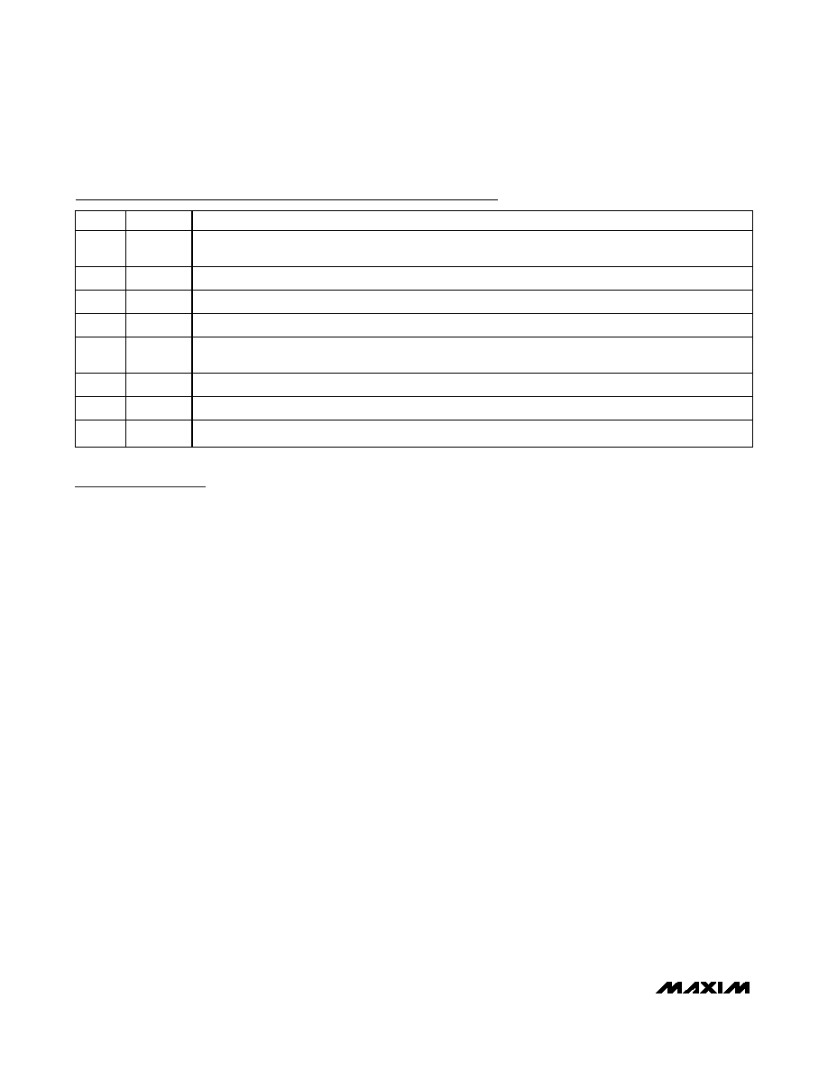
PIN
NAME
FUNCTION
13
SCLK
Serial Data Clock Input. Serial data on DIN is loaded on the rising edge of SCLK, and serial data is updated
on DOUT on the falling edge of SCLK. In external clock mode, SCLK sets the conversion speed.
14
DGND
Digital Ground. Connect to pin 5.
15
DVDD
Digital Supply. 5V ±5%. Bypass DVDD to DGND (pin 14) with a 0.1F capacitor.
16
DIN
Serial Data Input. Serial data on DIN is latched on the rising edge of SCLK.
17
CS
Chip-Select Input. Drive
CS low to enable the serial interface. When CS is high, DOUT is high impedance.
In external clock mode, SSTRB is high impedance when
CS is high.
18
CREF
Reference Buffer Bypass. Bypass CREF to AGND (pin 3) with 1F.
19
AGND
Analog Ground. Connect pin 19 to pin 3.
20
AIN
Analog Input
Pin Description (continued)
相关PDF资料 |
PDF描述 |
|---|---|
| HCM10DRTI-S13 | CONN EDGECARD 20POS .156 EXTEND |
| AC2626K4 | PROBE TEMP 4" GENERAL PURP |
| HBM10DRTI-S13 | CONN EDGECARD 20POS .156 EXTEND |
| 0210490252 | CABLE JUMPER 1.25MM .254M 18POS |
| ADZS-AUDIO-EX3 | BOARD EXTENDER AUDIO EI3 |
相关代理商/技术参数 |
参数描述 |
|---|---|
| MAX1132EVSYS | 制造商:MAXIM 制造商全称:Maxim Integrated Products 功能描述:Evaluation System for the MAX1132/MAX1133 |
| MAX1132-MAX1133 | 制造商:MAXIM 制造商全称:Maxim Integrated Products 功能描述:16-Bit ADC, 200ksps, 5V Single-Supply with Reference |
| MAX1133 | 制造商:MAXIM 制造商全称:Maxim Integrated Products 功能描述:16-Bit ADC, 200ksps, 5V Single-Supply with Reference |
| MAX11330 | 制造商:MAXIM 制造商全称:Maxim Integrated Products 功能描述:3Msps, 12-/10-Bit, 8-/16-Channel ADCs with Post-Mux External Signal Conditioning Access |
| MAX11330ATJ | 制造商:MAXIM 制造商全称:Maxim Integrated Products 功能描述:3Msps, 12-/10-Bit, 8-/16-Channel ADCs with Post-Mux External Signal Conditioning Access |
发布紧急采购,3分钟左右您将得到回复。