- 您现在的位置:买卖IC网 > PDF目录9899 > MAX1300BEUG+T (Maxim Integrated Products)IC ADC 16BIT SPI/SRL 24TSSOP PDF资料下载
参数资料
| 型号: | MAX1300BEUG+T |
| 厂商: | Maxim Integrated Products |
| 文件页数: | 18/31页 |
| 文件大小: | 0K |
| 描述: | IC ADC 16BIT SPI/SRL 24TSSOP |
| 产品培训模块: | Lead (SnPb) Finish for COTS Obsolescence Mitigation Program |
| 标准包装: | 2,500 |
| 位数: | 16 |
| 采样率(每秒): | 115k |
| 数据接口: | MICROWIRE?,QSPI?,串行,SPI? |
| 转换器数目: | 1 |
| 功率耗散(最大): | 976mW |
| 电压电源: | 模拟和数字 |
| 工作温度: | -40°C ~ 85°C |
| 安装类型: | 表面贴装 |
| 封装/外壳: | 24-TSSOP(0.173",4.40mm 宽) |
| 供应商设备封装: | 24-TSSOP |
| 包装: | 带卷 (TR) |
| 输入数目和类型: | 8 个单端,单极;8 个单端,双极;4 个差分,双极 |
第1页第2页第3页第4页第5页第6页第7页第8页第9页第10页第11页第12页第13页第14页第15页第16页第17页当前第18页第19页第20页第21页第22页第23页第24页第25页第26页第27页第28页第29页第30页第31页
External-Acquisition-Mode Control Byte
Internal-Clock-Mode Control Byte
Reset Byte
Partial Power-Down-Mode Control Byte
This prevents the MAX1300/MAX1301 from inadvertent-
ly exiting full power-down mode because of a CS glitch
in a noisy digital environment.
Power-On Reset
The MAX1300/MAX1301 power up in normal operation
configured for external clock mode with all circuitry
active (Tables 7 and 8). Each analog input channel
(CH0–CH7) is set for single-ended conversions with a
±3 x VREF bipolar input range (Table 6).
Allow the power supplies to stabilize after power-up. Do
not initiate any conversions until the power supplies
have stabilized. Additionally, allow 10ms for the internal
reference to stabilize when CREF = 1.0F and CREFCAP
= 0.1F. Larger reference capacitors require longer
stabilization times.
Internal or External Reference
The MAX1300/MAX1301 operate with either an internal or
external reference. The reference voltage impacts the
ADC’s FSR (Figures 12, 13, and 14). An external refer-
ence is recommended if more accuracy is required than
the internal reference provides, and/or multiple converters
require the same reference voltage.
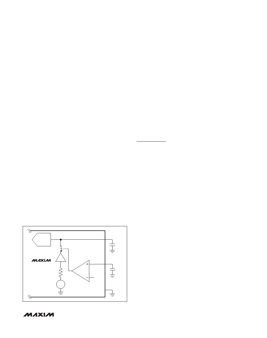
Internal Reference
The MAX1300/MAX1301 contain an internal 4.096V
bandgap reference. This bandgap reference is connect-
ed to REFCAP through a nominal 5k
resistor (Figure 17).
The voltage at REFCAP is buffered creating 4.096V at
REF. When using the internal reference, bypass
REFCAP with a 0.1F or greater capacitor to AGND1 and
bypass REF with a 1.0F or greater capacitor to AGND1.
External Reference
For external reference operation, disable the internal
reference and reference buffer by connecting REFCAP
to AVDD1. With AVDD1 connected to REFCAP, REF
becomes a high-impedance input and accepts an
external reference voltage. The MAX1300/MAX1301
can accept an external reference voltage of 4.096V or
less. However, to meet all of the electrical characteristic
specifications, VREF must be > 38V. The MAX1300/
MAX1301 external reference current varies depending
on the applied reference voltage and the operating
mode (see the External Reference Input Current vs.
External Reference Input Voltage in the
Typical
Operating Characteristics).
Applications Information
Noise Reduction
Additional samples can be taken and averaged (over-
sampling) to remove the effect of transition noise on
conversion results. The square root of the number of
samples determines the improvement in performance.
For example, with 2/3LSBRMS (4LSBP-P) transition
noise, 16 (42 = 16) samples must be taken to reduce
the noise to 1LSBP-P.
Interface with 0 to 10V Signals
In industrial control applications, 0 to 10V signaling is
common. For 0 to 10V applications, configure the selected
MAX1300/MAX1301 input channel for the single-ended 0
to 3 x VREF input range (R[2:0] = 110, Table 6). The 0 to
3x VREF range accommodates 0 to 10V where the sig-
nals saturate at approximately 3 x VREF if out of range.
Interface with 4–20mA Signals
Figure 19 illustrates a simple interface between the
MAX1300/MAX1301 and a 4–20mA signal. 4–20mA sig-
naling can be used as a binary switch (4mA represents
a logic-low signal, 20mA represents a logic-high sig-
nal), or for precision communication where currents
between 4mA and 20mA represent intermediate analog
data. For binary switch applications, connect the
4–20mA signal to the MAX1300/MAX1301 with a resis-
tor to ground. For example, a 250
resistor converts
the 4–20mA signal to a 1V to 5V signal. Adjust the
resistor value so the parallel combination of the resistor
and the MAX1300/MAX1301 source impedance is
250
. In this application, select the single-ended 0 to
(3 x VREF)/2 range (R[2:0] = 011, Table 6). For applica-
tions that require precision measurements of continu-
ous analog currents between 4mA and 20mA, use a
buffer to prevent the MAX1300/MAX1301 input from
diverting current from the 4–20mA signal.
MAX1300/MAX1301
8- and 4-Channel, ±3 x VREF Multirange Inputs,
Serial 16-Bit ADCs
______________________________________________________________________________________
25
REF
REFCAP
AGND1
4.096V
BANDGAP
REFERENCE
5k
1x
SAR
ADC REF
4.096V
1.0
F
0.1
F
VRCTH
MAX1300
MAX1301
Figure 17. Internal Reference Operation
相关PDF资料 |
PDF描述 |
|---|---|
| MS27499E22B35PA | CONN RCPT 100POS BOX MNT W/PINS |
| D38999/24MD19PA | CONN RCPT 19POS JAM NUT W/PINS |
| PT02SE-22-55S | CONN RECEPT 55POS W/SOCKET CRIMP |
| ISL32274EIVZ | IC XMITTER ESD RS422 LP 16-TSSOP |
| MS3111F14-5PY | CONN RCPT 5POS CBL MNT W/PINS |
相关代理商/技术参数 |
参数描述 |
|---|---|
| MAX1300EVKIT+ | 功能描述:数据转换 IC 开发工具 MAX1300 Eval Kit RoHS:否 制造商:Texas Instruments 产品:Demonstration Kits 类型:ADC 工具用于评估:ADS130E08 接口类型:SPI 工作电源电压:- 6 V to + 6 V |
| MAX13013EBT | 制造商:Rochester Electronics LLC 功能描述: 制造商:Maxim Integrated Products 功能描述: |
| MAX13013EBT+T | 功能描述:转换 - 电压电平 RoHS:否 制造商:Micrel 类型:CML/LVDS/LVPECL to LVCMOS/LVTTL 传播延迟时间:1.9 ns 电源电流:14 mA 电源电压-最大:3.6 V 电源电压-最小:3 V 最大工作温度:+ 85 C 安装风格:SMD/SMT 封装 / 箱体:MLF-8 |
| MAX13013EBT-T | 功能描述:转换 - 电压电平 RoHS:否 制造商:Micrel 类型:CML/LVDS/LVPECL to LVCMOS/LVTTL 传播延迟时间:1.9 ns 电源电流:14 mA 电源电压-最大:3.6 V 电源电压-最小:3 V 最大工作温度:+ 85 C 安装风格:SMD/SMT 封装 / 箱体:MLF-8 |
| MAX13013EXT | 制造商:Maxim Integrated Products 功能描述:+1.2V TO 3.6V 0.1MICROAMPS 100MBP - Cut Tape Product |
发布紧急采购,3分钟左右您将得到回复。