参数资料
| 型号: | MAX1400CAI+ |
| 厂商: | Maxim Integrated Products |
| 文件页数: | 6/34页 |
| 文件大小: | 0K |
| 描述: | IC ADC 18BIT LP 28-SSOP |
| 产品培训模块: | Lead (SnPb) Finish for COTS Obsolescence Mitigation Program |
| 标准包装: | 46 |
| 位数: | 18 |
| 采样率(每秒): | 480 |
| 数据接口: | QSPI?,串行,SPI? |
| 转换器数目: | 1 |
| 功率耗散(最大): | 1.25mW |
| 电压电源: | 模拟和数字 |
| 工作温度: | 0°C ~ 70°C |
| 安装类型: | 表面贴装 |
| 封装/外壳: | 28-SSOP(0.209",5.30mm 宽) |
| 供应商设备封装: | 28-SSOP |
| 包装: | 管件 |
| 输入数目和类型: | 3 个差分,单极;3 个差分,双极;5 个伪差分,单极;5 个伪差分,双极 |
第1页第2页第3页第4页第5页当前第6页第7页第8页第9页第10页第11页第12页第13页第14页第15页第16页第17页第18页第19页第20页第21页第22页第23页第24页第25页第26页第27页第28页第29页第30页第31页第32页第33页第34页
MAX1400
+5V, 18-Bit, Low-Power, Multichannel,
Oversampling (Sigma-Delta) ADC
14
______________________________________________________________________________________
FSYNC: (Default = 0) Filter Sync Bit. When FSYNC = 0,
conversions are automatically performed at a data rate
determined by CLK, FS1, FS0, MF1, and MF0 bits.
When FSYNC = 1, the digital filter and analog modulator
are held in reset, inhibiting normal self-timed operation.
This bit may be used to convert on command to mini-
mize the settling time to valid output data, or to synchro-
nize operation of a number of MAX1400s. FSYNC does
not reset the serial interface or the 0/DRDY flag. To clear
the 0/DRDY flag while FSYNC is active, simply read the
data register.
Global Setup Register 1
A1, A0: (Default = 0, 0) Channel-Selection Control Bits.
These bits (combined with the state of the DIFF, M1,
and M0 bits) determine the channel selected for con-
version according to Tables 8, 9, and 10. These bits
are ignored if the SCAN bit is set.
MF1, MF0: (Default = 0, 0) Modulator Frequency Bits.
MF1 and MF0 determine the ratio of CLKIN oscillator fre-
quency to modulator operating frequency. They affect
the output data rate, the position of the digital filter notch
frequencies, and the power dissipation of the device.
Achieve lowest power dissipation with MF1 = 0 and MF0
= 0. Highest power dissipation and fastest output data
rate occur with these bits set to 1, 1 (Table 2).
CLK: (Default = 1) CLK Bit. The CLK bit is used in con-
junction with X2CLK to tell the MAX1400 the frequency
of the CLKIN input signal. If CLK = 0, a CLKIN input fre-
quency of 1.024MHz (2.048MHz for X2CLK = 1) is
expected. If CLK = 1, a CLKIN input frequency of
2.4576MHz (4.1952MHz for X2CLK = 1) is expected.
This bit affects the decimation factor in the digital filter
and thus the output data rate (Table 2).
FS1, FS0: (Default = 0, 1) Filter Selection Bits. These
bits (in conjunction with the CLK bit) control the deci-
mation ratio of the digital filter. They determine the out-
put data rate, the position of the digital filter-frequency
response notches, and the noise present in the output
result. (Table 2).
FAST: (Default 0) FAST Bit. FAST = 0 causes the digi-
tal filter to perform a SINC3 filter function on the modu-
lator data stream. The output data rate will be
determined by the values in the CLK, FS1, FS0, MF1,
and MF0 bits (Table 2). The settling time for SINC3
function is 3 [1 / (output data rate)]. In SINC3 mode, the
MAX1400 automatically holds the DRDY signal false
(after any significant configuration change) until settled
data is available. FAST = 1 causes the digital filter to
perform a SINC1 filter function on the modulator data
stream. The signal-to-noise ratio achieved with this filter
function is less than that of the SINC3 filter; however
SINC1 settles in a single output sample period, rather
than a minimum of three output sample periods for
SINC3. When switching from SINC1 to SINC3 mode, the
DRDY flag will be deasserted and reasserted after the
filter has fully settled. This mode change requires a
minimum of three samples.
Global Setup Register 2
SCAN: (Default = 0) Scan Bit. Setting this bit to a 1
causes sequential scanning of the input channels as
determined by DIFF, M1, and M0 (see Scanning
(SCAN-mode) section). When SCAN = 0, the MAX1400
repeatedly measures the unique channel selected by
A1, A0, DIFF, M1, and M0.
M1, M0: (Default 0, 0) Mode Control Bits. These bits
control access to the calibration channels CALOFF and
CALGAIN. When SCAN = 0, setting M1 = 0 and M0 = 1
selects the CALOFF input, and M1 = 1 and M0 = 0
selects the CALGAIN input (Table 3). When SCAN = 1
and M1
≠ M0, the scanning sequence includes both
CALOFF and CALGAIN inputs (Table 4). When SCAN is
set to 1 and the device is scanning the available input
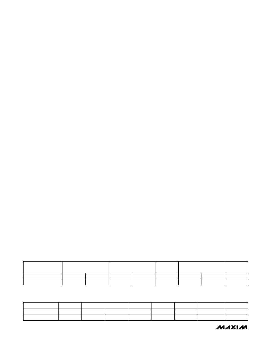
First Bit (MSB)
(LSB)
First Bit (MSB)
(LSB)
A1
CLK
0
1
A0
Defaults
CHANNEL SELECTION
0
MF1
0
MF0
MODULATOR
FREQUENCY
0
FAST
Name
0
FS1
0
FS0
FILTER SELECTION
1
FUNCTION
SCAN
DIFF
0
M1
Defaults
0
M0
0
BUFF
MODE CONTROL
0
X2CLK
Name
0
BOUT
0
RESERVED
0
FUNCTION
Global Setup Register 2
Global Setup Register 1
相关PDF资料 |
PDF描述 |
|---|---|
| MAX1401CAI+ | IC ADC 18BIT LP 28-SSOP |
| MAX1415AEWE+T | IC ADC 16BIT DELTA SIGMA 16-SOIC |
| MAX1421CCM+D | IC ADC 12BIT 40MSPS 48LQFP |
| MAX1426EAI+T | IC ADC 10BITS 10MSPS 28SSOP |
| MAX1434ECQ+D | IC ADC 10BIT 50MSPS 100-TQFP |
相关代理商/技术参数 |
参数描述 |
|---|---|
| MAX1400CAI+ | 功能描述:模数转换器 - ADC 18-Bit 5Ch 4.8ksps 2.5V Precision ADC RoHS:否 制造商:Texas Instruments 通道数量:2 结构:Sigma-Delta 转换速率:125 SPs to 8 KSPs 分辨率:24 bit 输入类型:Differential 信噪比:107 dB 接口类型:SPI 工作电源电压:1.7 V to 3.6 V, 2.7 V to 5.25 V 最大工作温度:+ 85 C 安装风格:SMD/SMT 封装 / 箱体:VQFN-32 |
| MAX1400CAI+T | 功能描述:模数转换器 - ADC 18-Bit 5Ch 4.8ksps 2.5V Precision ADC RoHS:否 制造商:Texas Instruments 通道数量:2 结构:Sigma-Delta 转换速率:125 SPs to 8 KSPs 分辨率:24 bit 输入类型:Differential 信噪比:107 dB 接口类型:SPI 工作电源电压:1.7 V to 3.6 V, 2.7 V to 5.25 V 最大工作温度:+ 85 C 安装风格:SMD/SMT 封装 / 箱体:VQFN-32 |
| MAX1400CAI+W | 制造商:Maxim Integrated Products 功能描述: |
| MAX1400CAI-T | 功能描述:模数转换器 - ADC RoHS:否 制造商:Texas Instruments 通道数量:2 结构:Sigma-Delta 转换速率:125 SPs to 8 KSPs 分辨率:24 bit 输入类型:Differential 信噪比:107 dB 接口类型:SPI 工作电源电压:1.7 V to 3.6 V, 2.7 V to 5.25 V 最大工作温度:+ 85 C 安装风格:SMD/SMT 封装 / 箱体:VQFN-32 |
| MAX1400EAI | 功能描述:模数转换器 - ADC RoHS:否 制造商:Texas Instruments 通道数量:2 结构:Sigma-Delta 转换速率:125 SPs to 8 KSPs 分辨率:24 bit 输入类型:Differential 信噪比:107 dB 接口类型:SPI 工作电源电压:1.7 V to 3.6 V, 2.7 V to 5.25 V 最大工作温度:+ 85 C 安装风格:SMD/SMT 封装 / 箱体:VQFN-32 |
发布紧急采购,3分钟左右您将得到回复。