参数资料
| 型号: | MAX1401EAI+T |
| 厂商: | Maxim Integrated Products |
| 文件页数: | 3/36页 |
| 文件大小: | 0K |
| 描述: | IC ADC 18BIT LP 28-SSOP |
| 产品培训模块: | Lead (SnPb) Finish for COTS Obsolescence Mitigation Program |
| 标准包装: | 2,000 |
| 位数: | 18 |
| 采样率(每秒): | 480 |
| 数据接口: | QSPI?,串行,SPI? |
| 转换器数目: | 1 |
| 功率耗散(最大): | 750µW |
| 电压电源: | 模拟和数字 |
| 工作温度: | -40°C ~ 85°C |
| 安装类型: | 表面贴装 |
| 封装/外壳: | 28-SSOP(0.209",5.30mm 宽) |
| 供应商设备封装: | 28-SSOP |
| 包装: | 带卷 (TR) |
| 输入数目和类型: | 3 个差分,单极;3 个差分,双极;5 个伪差分,单极;5 个伪差分,双极 |
第1页第2页当前第3页第4页第5页第6页第7页第8页第9页第10页第11页第12页第13页第14页第15页第16页第17页第18页第19页第20页第21页第22页第23页第24页第25页第26页第27页第28页第29页第30页第31页第32页第33页第34页第35页第36页
MAX1401
+3V, 18-Bit, Low-Power, Multichannel,
Oversampling (Sigma-Delta) ADC
______________________________________________________________________________________
11
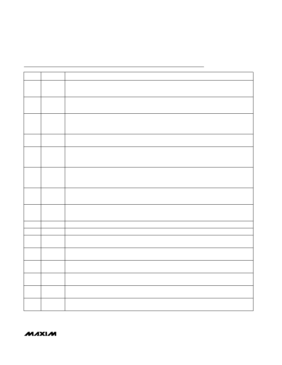
Pin Description
Analog Input 6. May be used as a common point for AIN1 through AIN5 in pseudo-differential mode, or as
the negative input of the AIN5/AIN6 differential analog input pair (see On-Chip Registers section).
AIN6
16
Analog Input Channel 4. May be used as a pseudo-differential input with AIN6 as common, or as the neg-
ative input of the AIN3/AIN4 differential analog input pair (see On-Chip Registers section).
AIN4
14
Analog Input Channel 3. May be used as a pseudo-differential input with AIN6 as common, or as the posi-
tive input of the AIN3/AIN4 differential analog input pair (see On-Chip Registers section).
AIN3
13
Analog Input Channel 2. May be used as a pseudo-differential input with AIN6 as common, or as the neg-
ative input of the AIN1/AIN2 differential analog input pair (see On-Chip Registers section).
AIN2
12
Analog Input Channel 1. May be used as a pseudo-differential input with AIN6 as common, or as the posi-
tive input of the AIN1/AIN2 differential analog input pair (see On-Chip Registers section).
AIN1
11
Analog Positive Supply Voltage (+2.7V to +3.6V)
V+
10
Analog Ground. Reference point for the analog circuitry. AGND connects to the IC substrate.
AGND
9
Negative Analog Input. A direct input to the negative buffer and the negative differential input terminal of
the ADC - bypassing the input mux. This signal forms a differential input pair with ADCIN+. Connect
ADCIN- to MUXOUT- when direct access is not required.
ADCIN-
8
Positive Analog Input. A direct input to the positive buffer and the positive differential input terminal of the
ADC, bypassing the input mux. This signal forms a differential input pair with ADCIN-. Connect ADCIN+ to
MUXOUT+ when direct access is not required.
ADCIN+
7
Negative Analog Mux Output. The negative differential output signal from the part’s internal input multi-
plexer. Use this signal in conjunction with MUXOUT+ and a high-quality external amplifier for additional
signal processing before conversion. Return the processed output through ADCIN+ and ADCIN-.
Connect MUXOUT- directly to ADCIN- if external processing is not required.
MUXOUT-
6
Positive Analog Mux Output. The positive differential output signal from the part’s internal input multiplex-
er. Use this signal in conjunction with MUXOUT- and a high-quality external amplifier for additional signal
processing before conversion. Return the processed output through ADCIN+ and ADCIN-. Connect
MUXOUT+ directly to ADCIN+ if external processing is not required.
MUXOUT+
5
Active-Low Reset Input. Drive low to reset the control logic, interface logic, digital filter, and analog modu-
lator to power-on status. RESET must be high and CLKIN must be toggling in order to exit reset.
RESET
4
Chip-Select Input. This active-low logic input is used to enable the digital interface. With CS hard-wired
low, the MAX1401 operates in its 3-wire interface mode with SCLK, DIN, and DOUT used to interface to
the device. CS is used either to select the device in systems with more than one device on the serial bus,
or as a frame-synchronization signal for the MAX1401 when a continuous SCLK is used.
CS
3
Clock Output. When deriving the master clock from a crystal, connect the crystal between CLKIN and
CLKOUT. In this mode, the on-chip clock signal is not available at CLKOUT. Leave CLKOUT unconnected
when CLKIN is driven with an external clock.
CLKOUT
2
PIN
Clock Input. A crystal can be connected across CLKIN and CLKOUT. Alternatively, drive CLKIN with a
CMOS-compatible clock at a nominal frequency of 2.4576MHz or 1.024MHz, and leave CLKOUT uncon-
nected. Frequencies of 4.9152MHz and 2.048MHz may be used if the X2CLK control bit is set to 1.
CLKIN
1
FUNCTION
NAME
Analog Input Channel 5. Used as a differential or pseudo-differential input with AIN6 (see On-Chip
Registers section).
AIN5
15
相关PDF资料 |
PDF描述 |
|---|---|
| V24B5M150BG | CONVERTER MOD DC/DC 5V 150W |
| MS3102R36-15S | CONN RCPT 35POS BOX MNT W/SCKT |
| MAX1189CCUI+ | IC ADC 16BIT 135KSPS 28-TSSOP |
| MS3102E36-15S | CONN RCPT 35POS BOX MNT W/SCKT |
| MS27505E11F13P | CONN RCPT 13POS BOX MNT W/PINS |
相关代理商/技术参数 |
参数描述 |
|---|---|
| MAX1402CAI | 功能描述:ADC / DAC多通道 RoHS:否 制造商:Texas Instruments 转换速率: 分辨率:8 bit 接口类型:SPI 电压参考: 电源电压-最大:3.6 V 电源电压-最小:2 V 最大工作温度:+ 85 C 安装风格:SMD/SMT 封装 / 箱体:VQFN-40 |
| MAX1402CAI+ | 功能描述:模数转换器 - ADC 18-Bit 5Ch 4.8ksps 2.5V Precision ADC RoHS:否 制造商:Texas Instruments 通道数量:2 结构:Sigma-Delta 转换速率:125 SPs to 8 KSPs 分辨率:24 bit 输入类型:Differential 信噪比:107 dB 接口类型:SPI 工作电源电压:1.7 V to 3.6 V, 2.7 V to 5.25 V 最大工作温度:+ 85 C 安装风格:SMD/SMT 封装 / 箱体:VQFN-32 |
| MAX1402CAI+T | 功能描述:模数转换器 - ADC 18-Bit 5Ch 4.8ksps 2.5V Precision ADC RoHS:否 制造商:Texas Instruments 通道数量:2 结构:Sigma-Delta 转换速率:125 SPs to 8 KSPs 分辨率:24 bit 输入类型:Differential 信噪比:107 dB 接口类型:SPI 工作电源电压:1.7 V to 3.6 V, 2.7 V to 5.25 V 最大工作温度:+ 85 C 安装风格:SMD/SMT 封装 / 箱体:VQFN-32 |
| MAX1402CAI-T | 功能描述:ADC / DAC多通道 RoHS:否 制造商:Texas Instruments 转换速率: 分辨率:8 bit 接口类型:SPI 电压参考: 电源电压-最大:3.6 V 电源电压-最小:2 V 最大工作温度:+ 85 C 安装风格:SMD/SMT 封装 / 箱体:VQFN-40 |
| MAX1402EAI | 功能描述:ADC / DAC多通道 RoHS:否 制造商:Texas Instruments 转换速率: 分辨率:8 bit 接口类型:SPI 电压参考: 电源电压-最大:3.6 V 电源电压-最小:2 V 最大工作温度:+ 85 C 安装风格:SMD/SMT 封装 / 箱体:VQFN-40 |
发布紧急采购,3分钟左右您将得到回复。